Types of I/O Buses
Since the introduction of the
first PC, many I/O buses have been introduced. The reason is simple: Faster I/O
speeds are necessary for better system performance. This need for higher
performance involves three main areas:
·
Faster CPUs
·
Increasing
software demands
·
Greater
multimedia requirements
Each of these areas requires
the I/O bus to be as fast as possible.
One of the primary reasons new
I/O bus structures have been slow in coming is compatibility that old catch-22
that anchors much of the PC industry to the past. One of the hallmarks of the
PC's success is its standardization. This standardization spawned thousands of
third-party I/O cards, each originally built for the early bus specifications
of the PC. If a new high-performance bus system was introduced, it often had to
be compatible with the older bus systems so the older I/O cards would not be
obsolete. Therefore, bus technologies seem to evolve rather than make quantum
leaps forward.
You can identify different
types of I/O buses by their architectures. The main types of I/O buses are
detailed earlier in this chapter.
The main differences among
buses consist primarily of the amounts of data they can transfer at one time
and the speeds at which they can do it. The following sections describe the
various types of PC buses.
The ISA Bus
Industry Standard Architecture
(ISA) is the bus architecture that was introduced as an 8-bit bus with the
original IBM PC in 1981; it was later expanded to 16 bits with the IBM PC/AT in
1984. ISA is the basis of the modern personal computer and the primary
architecture used in the vast majority of PC systems on the market today. It
might seem amazing that such a presumably antiquated architecture is used in
today's high-performance systems, but this is true for reasons of reliability,
affordability, and compatibility, plus this old bus is still faster than many
of the peripherals we connect to it!
Two versions of the ISA bus
exist, based on the number of data bits that can be transferred on the bus at a
time. The older version is an 8-bit bus; the newer version is a 16-bit bus. The
original 8-bit version ran at 4.77MHz in the PC and XT, and the 16-bit version
used in the AT ran at 6MHz and then 8MHz. Later, the industry as a whole agreed
on an 8.33MHz maximum standard speed for 8/16-bit versions of the ISA bus for
backward-compatibility. Some systems have the capability to run the ISA bus
faster than this, but some adapter cards will not function properly at higher
speeds. ISA data transfers require anywhere from two to eight cycles.
Therefore, the theoretical maximum data rate of the ISA bus is about 8MBps, as
the following formula shows:
8.33MHz x 2 bytes (16 bits) ÷
2 cycles per transfer = 8.33MBps
The bandwidth of the 8-bit bus
would be half this figure (4.17MBps). Remember, however, that these figures are
theoretical maximums. Because of I/O bus protocols, the effective bandwidth is
much lower—typically by almost half. Even so, at
about 8MBps, the ISA bus is still faster than many of the peripherals connected
to it, such as serial ports, parallel ports, floppy controllers, keyboard
controllers, and so on.
The 8-Bit ISA Bus
This bus architecture is used
in the original IBM PC computers and was retained for several years in later
systems. Although virtually nonexistent in new systems today, this architecture
still exists in hundreds of thousands of PC systems in the field.
Physically, the 8-bit ISA expansion
slot resembles the tongue-and-groove system furniture makers once used to hold
two pieces of wood together. It is specifically called a card/edge connector. An adapter card with 62 contacts
on its bottom edge plugs into a slot on the motherboard that has 62 matching
contacts. Electronically, this slot provides 8 data lines and 20 addressing
lines, enabling the slot to handle 1MB of memory.
Figure 1 describes the pinouts for the 8-bit ISA bus; Figure 2 shows how these
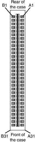
pins are oriented in the expansion slot.
Figure 1. Pinouts for the 8-bit ISA bus.
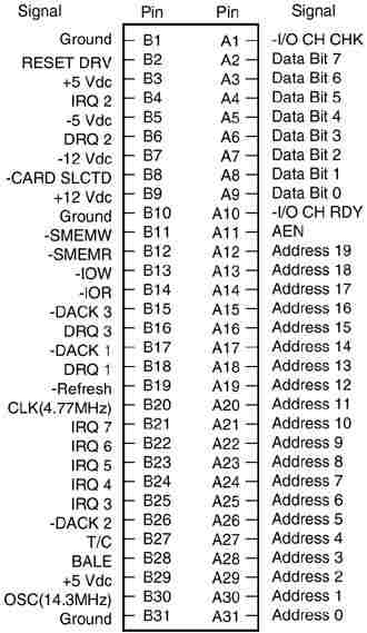
Figure 2. The 8-bit ISA bus connector.
Although the design of the bus
is simple, IBM waited until 1987 to publish full specifications for the timings
of the data and address lines, so in the early days of PC compatibles,
manufacturers had to do their best to figure out how to make adapter boards.
This problem was solved, however, as PC-compatible personal computers became
more widely accepted as the industry standard and manufacturers had more time
and incentive to build adapter boards that worked correctly with the bus.
The dimensions of 8-bit ISA
adapter cards are as follows:
4.2'' (106.68mm) high
13.13'' (333.5mm) long
The 16-Bit ISA
Bus
IBM threw a bombshell on the
PC world when it introduced the AT with the 286 processor in 1984. This
processor had a 16-bit data bus, which meant communications between the
processor and motherboard as well as memory would now be 16 bits wide instead
of only 8. Although this processor could have been installed on a motherboard
with only an 8-bit I/O bus, that would have meant a huge sacrifice in the
performance of any adapter cards or other devices installed on the bus.
Rather than create a new I/O
bus, at that time IBM instead came up with a system that could support both 8-
and 16-bit cards by retaining the same basic 8-bit connector layout but adding
an optional 16-bit extension connector. This first debuted on the PC/AT in
August 1984, which is why we also refer to the ISA bus as the AT-bus.
The extension connector in
each 16-bit expansion slot adds 36 connector pins (for a total of 96 signals)
to carry the extra signals necessary to implement the wider data path. In
addition, two of the pins in the 8-bit portion of the connector were changed.
These two minor changes did not alter the function of 8-bit cards.
Figure 3 describes the pinouts for the full 16-bit ISA expansion slot, and Figure 4
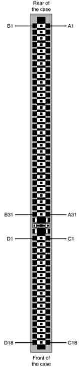
shows how the additional pins are oriented in the expansion slot.
Figure 3. Pinouts for the 16-bit ISA bus.
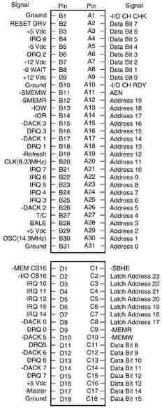
Figure 4. The ISA 16-bit bus connector.
Because of physical
interference with some ancient 8-bit card designs, IBM left 16-bit extension
connectors off two of the slots in the AT. This was not a problem in newer
systems, so any system with ISA slots would have all of them as full 16-bit
versions.
The dimensions of a typical AT
expansion board are as follows:
4.8'' (121.92mm) high
13.13'' (333.5mm) long
0.5'' (12.7mm) wide
Two heights actually are
available for cards commonly used in AT systems: 4.8'' and 4.2'' (the height of
older PC-XT cards). The shorter cards became an issue when IBM introduced the
XT Model 286. Because this model has an AT motherboard in an XT case, it needs
AT-type boards with the 4.2'' maximum height. Most board makers trimmed the
height of their boards; most manufacturers who still make ISA cards now make
only 4.2'' tall (or less) boards so they will work in systems with either
profile.
32-Bit Buses
After 32-bit CPUs became
available, it was some time before 32-bit bus standards became available.
Before MCA and EISA specs were released, some vendors began creating their own
proprietary 32-bit buses, which were extensions of the ISA bus. Fortunately,
these proprietary buses were few and far between.
The expanded portions of the
bus typically are used for proprietary memory expansion or video cards. Because
the systems are proprietary (meaning that they are nonstandard), pinouts and specifications are not available.
The Micro Channel
Bus
The introduction of 32-bit
chips meant that the ISA bus could not handle the power of another new
generation of CPUs. The 386DX chips could transfer 32 bits of data at a time,
but the ISA bus can handle a maximum of only 16 bits. Rather than extend the
ISA bus again, IBM decided to build a new bus; the result was the MCA bus. MCA (an abbreviation for microchannel
architecture) is completely different from the ISA bus and is technically
superior in every way.
IBM wanted not only to replace
the old ISA standard, but also to require vendors to license certain parts of
the technology. Many owed for licenses on the ISA bus technology that IBM also
created, but because IBM had not been aggressive in its licensing of ISA, many
got away without any license. Problems with licensing and control led to the
development of the competing EISA bus (see the next section on the EISA bus)
and hindered acceptance of the MCA bus.
MCA systems produced a new
level of ease of use; they were plug-and-play before the official Plug and Play
specification even existed. An MCA system had no jumpers and switches—neither on the motherboard nor
on any expansion adapter. Instead you used a special Reference disk, which went
with the particular system, and Option disks, which went with each of the cards
installed in the system. After a card was installed, you loaded the Option disk
files onto the Reference disk; after that, you didn't need the Option disks
anymore. The Reference disk contained the special BIOS and system setup program
necessary for an MCA system, and the system couldn't be configured without it.
To support older PS/2 systems, IBM maintains a library of all its Reference and
Options disks at ftp://ftp.pc.ibm.com/pub/pccbbs.
Check this site if you are supporting any old MCA-based systems and need any of
these files.
For more information on the
MCA bus, see the previous editions of this book on the included DVD-ROM.
The EISA Bus
The Extended Industry Standard
Architecture (EISA) standard was announced in September 1988 as a response to
IBM's introduction of the MCA bus more specifically, to the way IBM wanted to
handle licensing of the MCA bus. Vendors did not feel obligated to pay retroactive
royalties on the ISA bus, so they turned their backs on IBM and created their
own buses.
The EISA standard was
developed primarily by Compaq and was intended to be its way of taking over
future development of the PC bus from IBM. Compaq knew that nobody would clone
its bus if it was the only company that had it, so it essentially gave the design
to other leading manufacturers. Compaq formed the EISA committee, a nonprofit
organization designed specifically to control development of the EISA bus. Very
few EISA adapters were ever developed. Those that were developed centered
mainly around disk array controllers and server-type
network cards.
The EISA bus was essentially a
32-bit version of ISA. Unlike the MCA bus from IBM, you could still use older
8-bit or 16-bit ISA cards in 32-bit EISA slots, providing for full
backward-compatibility. As with MCA, EISA also allowed for automatic
configuration of EISA cards via software.
The EISA bus added 90 new
connections (55 new signals plus grounds) without increasing the physical
connector size of the 16-bit ISA bus. At first glance, the 32-bit EISA slot looks
a lot like the 16-bit ISA slot. The EISA adapter, however, has two rows of
stacked contacts. The first row is the same type used in 16-bit ISA cards; the
other, thinner row extends from the 16-bit connectors. Therefore, ISA cards can
still be used in EISA bus slots. Although this compatibility was not enough to
ensure the popularity of EISA buses, it is a feature that was carried over into
the VL-Bus standard that followed. The physical specifications of an EISA card
are as follows:
·
5'' (127mm) high
·
13.13''
(333.5mm) long
·
0.5'' (12.7mm)
wide
The EISA bus can handle up to
32 bits of data at an 8.33MHz cycle rate. Most data transfers require a minimum
of two cycles, although faster cycle rates are possible if an adapter card
provides tight timing specifications. The maximum bandwidth on the bus is
33MBps, as the following formula shows:
8.33MHz x 4 bytes (32 bits) =
33MBps
Figure 5 describes the pinouts for the EISA bus. Figure 6.
shows the locations of the pins; note how some pins
are offset to allow the EISA slot to accept ISA cards. Figure 7 shows the card
connector for the EISA expansion slot.
Figure 5. Pinouts for the EISA bus.
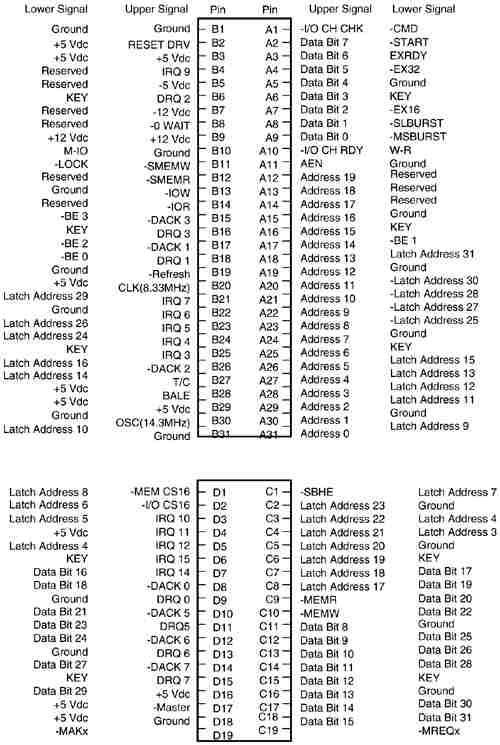
Figure 6. Pin locations inside the EISA bus connector.
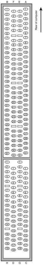
Figure 7. The EISA bus connector.
Local Buses
The I/O buses discussed so far
(ISA, MCA, and EISA) have one thing in common: relatively slow speed. The next
three bus types that are discussed in the following few sections all use the local bus concept explained in this section to address
the speed issue. The three main local buses found in PC systems are
·
VL-Bus (VESA
local bus)
·
PCI
·
AGP
The speed limitation of ISA,
MCA, and EISA is a carryover from the days of the original PC when the I/O bus
operated at the same speed as the processor bus. As the speed of the processor
bus increased, the I/O bus realized only nominal speed improvements, primarily
from an increase in the bandwidth of the bus. The I/O bus had to remain at a
slower speed because the huge installed base of adapter cards could operate
only at slower speeds.
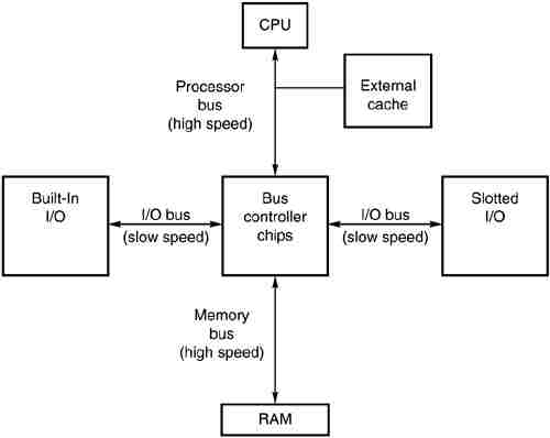
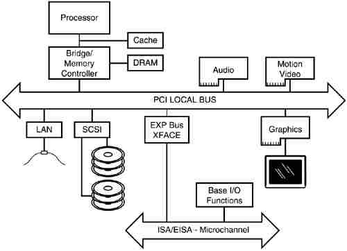
Figure 8 shows a conceptual
block diagram of the buses in a computer system.
Figure 8. Bus layout in a traditional PC.
The thought of a computer
system running more slowly than it could is very bothersome to some computer
users. Even so, the slow speed of the I/O bus is nothing more than a nuisance
in most cases. You don't need blazing speed to communicate with a keyboard or mouse—you gain nothing in performance. The real
problem occurs in subsystems in which you need the speed, such as video and
disk controllers.
The speed problem became acute
when graphical user interfaces (such as Windows) became prevalent. These
systems require the processing of so much video data that the I/O bus became a
literal bottleneck for the entire computer system. In other words, it did
little good to have a processor that was capable of 66MHz–450MHz or faster
if you could put data through the I/O bus at a rate of only 8MHz.
An obvious solution to this
problem is to move some of the slotted I/O to an area where it could access the
faster speeds of the processor bus—much the same
way as the external cache. Figure 9 shows this arrangement.
Figure 9. How a local bus works.

This arrangement became known
as local bus because external devices (adapter
cards) now could access the part of the bus that was local to the CPU—the processor bus. Physically, the slosts provided to tap this new configuration would need to
be different from existing bus slots to prevent adapter cards designed for
slower buses from being plugged into the higher bus speeds, which this design
made accessible.
It is interesting to note that
the very first 8-bit and 16-bit ISA buses were a form of local bus
architecture. These systems had the processor bus as the main bus, and
everything ran at full processor speeds. When ISA systems ran faster than 8MHz,
the main ISA bus had to be decoupled from the processor bus because expansion
cards, memory, and so on could not keep up. In 1992, an extension to the ISA
bus called the VESA local bus (VL-Bus) started showing up on PC systems,
indicating a return to local bus architecture. Since then, the peripheral
component interconnect (PCI) local bus has supplanted VL-Bus, and the AGP bus
has been introduced to complement PCI.
Local bus solutions do not
necessarily replace earlier standards, such as ISA; they are designed into the
system as a bus that is closer to the processor in the system architecture.
Older buses such as ISA were kept around for backward compatibility with slower
types of adapters that didn't need any faster connection to the system (such as
modems). Therefore, until recently a typical system might have AGP, PCI, and
ISA slots. Older cards still are compatible with such a system, but high-speed
adapter cards can take advantage of the AGP and PCI local bus slots as well.
With the demise of ISA slots and the movement of traditionally ISA-based
motherboard devices to the LPC interface, today's motherboards essentially use
other buses or dedicated interfaces for most of the connections that would have
previously used ISA.
The performance of graphical
user interfaces such as Windows and OS/2 have been tremendously improved by
moving the video cards off the slow ISA bus and onto faster PCI and now AGP
local buses.
VESA Local Bus
The Video Electronics
Standards Association (VESA) local bus was the most popular local bus design
from its debut in August 1992 through 1994. It was created by the VESA
committee, a nonprofit organization originally founded by NEC to further develop
video display and bus standards. In a similar fashion to how EISA evolved, NEC
had done most of the work on the VL-Bus (as it would be called) and, after
founding the nonprofit VESA committee, NEC turned over future development to
VESA. At first, the local bus slot seemed designed to be used primarily for
video cards. Improving video performance was a top priority at NEC to help sell
its high-end displays as well as its own PC systems. By 1991, video performance
had become a real bottleneck in most PC systems.
The VL-Bus can move data 32
bits at a time, enabling data to flow between the CPU and a compatible video
subsystem or hard drive at the full 32-bit data width of the 486 chip. The
maximum rated throughput of the VL-Bus is 133MBps. In other words, local bus
went a long way toward removing the major bottlenecks that existed in earlier
bus configurations.
Unfortunately, the VL-Bus did
not seem to be a long-lived concept. The design was simple indeed—just
take the pins from the 486 processor and run them out to a card connector
socket. So, the VL-Bus is essentially the raw 486 processor bus. This allowed a
very inexpensive design because no additional chipsets or interface chips were
required. A motherboard designer could add VL-Bus slots to its 486 motherboards
very easily and at a very low cost. This is why these slots appeared on
virtually all 486 system designs overnight.
Problems arose with timing
glitches caused by the capacitance introduced into the circuit by different
cards. Because the VL-Bus ran at the same speed as the processor bus, different
processor speeds meant different bus speeds, and full compatibility was
difficult to achieve. Although the VL-Bus could be adapted to other processors including
the 386 or even the Pentium—it was designed for
the 486 and worked best as a 486 solution only. Despite the low cost, after a
new bus called PCI appeared, VL-Bus fell into disfavor very quickly. It never
did catch on with Pentium systems, and there was little or no further
development of the VL-Bus in the PC industry.
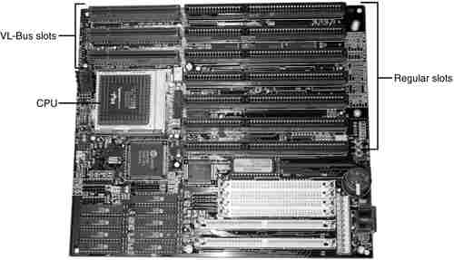
Physically, the VL-Bus slot
was an extension of the slots used for whatever type of base system you have.
If you have an ISA system, the VL-Bus is positioned as an extension of your
existing 16-bit ISA slots. Figure 11 shows how the VL-Bus slots are oriented on
a typical ISA/VL-Bus motherboard. The VESA extension has 112 contacts and uses
the same physical connector as the MCA bus.
Figure 11. An example of a typical
motherboard (albeit ancient) with VL-Bus slots.
The PCI Bus
In early 1992, Intel
spearheaded the creation of another industry group. It was formed with the same
goals as the VESA group in relation to the PC bus. Recognizing the need to
overcome weaknesses in the ISA and EISA buses, the PCI Special Interest Group
was formed.
The PCI bus specification was
released in June 1992 as version 1.0 and since then has undergone several
upgrades. Table shows the various releases of PCI.
PCI redesigned the traditional
PC bus by inserting another bus between the CPU and the native I/O bus by means
of bridges. Rather than tap directly into the processor bus, with its delicate
electrical timing (as was done in the VL-Bus), a new set of controller chips
was developed to extend the bus, as shown in Figure 11.
The PCI bus often is called a mezzanine bus because it adds another layer to the
traditional bus configuration. PCI bypasses the standard I/O bus; it uses the
system bus to increase the bus clock speed and take full advantage of the CPU's
data path. Systems that integrate the PCI bus became available in mid-1993 and
have since become a mainstay in the PC.
Information typically is
transferred across the PCI bus at 33MHz and 32 bits at a time. The bandwidth is
133MBps, as the following formula shows:
33.33MHz x 4 bytes (32 bits) =
133MBps
Although 32-bit 33MHz PCI is
the standard found in most PCs, there are now several variations on PCI as
shown in Table.
Table . PCI Bus Types
|
||||
|
PCI Bus Type |
Bus
Width (Bits) |
Bus
Speed (MHz) |
Data
Cycles per Clock |
Bandwidth
(MBps) |
|
PCI |
32 |
33 |
1 |
133 |
|
PCI 66MHz |
32 |
66 |
1 |
266 |
|
PCI 64-bit |
64 |
33 |
1 |
266 |
|
PCI 66MHz/64-bit |
64 |
66 |
1 |
533 |
|
PCI-X 64 |
64[*] |
66 |
1 |
533 |
|
PCI-X 133 |
64[*] |
133 |
1 |
1,066 |
|
PCI-X 266 |
64[*] |
133 |
2 |
2,132 |
|
PCI-X 533 |
64[*] |
133 |
4 |
4,266 |
|
PCI-Express[**] |
1 |
2,500 |
0.8 |
250 |
|
PCI-Express[**] |
32 |
2,500 |
0.8 |
8,000 |
[*] Bus width on PCI-X devices can be shared by multiple 32-bit
or 16-bit devices.
[**] PCI Express uses 8b/10b encoding, which transfers 8 bits for
every 10 bits sent and can transfer 1–32 bits at a time, depending on how
many lanes are in the implementation.
Currently, the 64-bit or 66MHz
and 133MHz variations are used only on server- or workstation-type boards and
systems. Aiding performance is the fact that the PCI bus can operate
concurrently with the processor bus; it does not supplant it. The CPU can be
processing data in an external cache while the PCI bus is busy transferring
information between other parts of the system—a
major design benefit of the PCI bus.
A PCI adapter card uses its
own unique connector. This connector can be identified within a computer system
because it typically is offset from the normal ISA, MCA, or EISA connectors
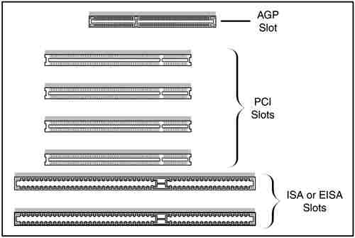
found in older motherboards. See Figure 12 for an example. The size of a PCI
card can be the same as that of the cards used in the system's normal I/O bus.
Figure 12. Typical configuration of 32-bit 33MHz PCI slots in
relation to ISA or EISA and AGP slots.
The PCI specification
identifies three board configurations, each designed for a specific type of
system with specific power requirements; each specification has a 32-bit
version and a longer 64-bit version. The 5V specification is for stationary
computer systems (using PCI 2.2 or earlier versions), the 3.3V specification is
for portable systems (also supported by PCI 2.3), and the universal
specification is for motherboards and cards that work in either type of system.
64-bit versions of the 5V and universal PCI slots are found primarily on server
motherboards. The PCI-X 2.0 specifications for 266 and 533 versions support
3.3V and 1.5V signaling; this corresponds to PCI version 2.3, which supports
3.3V signaling.
Note
The pinouts
for the 5V, 3.3V, and universal PCI slots can be found on the DVD-ROM in the
Technical Reference section. |
Figure 13 compares the 32-bit
and 64-bit versions of the standard 5V PCI slot to a 64-bit universal PCI slot.
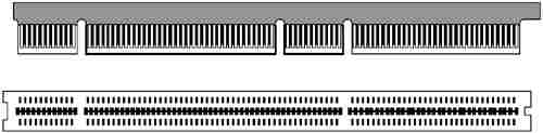
Figure 14 shows how the connector on a 64-bit universal PCI card compares to
the 64-bit universal PCI slot.
Figure 13. A 32-bit, 33MHz PCI slot (top) compared to a 64-bit
33MHz PCI slot (center) and a 64-bit universal PCI slot that runs at 66MHz
(bottom).
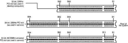
Figure 14. A 64-bit universal PCI card (top) compared to the
64-bit universal PCI slot (bottom).
Notice that the universal PCI
board specifications effectively combine the 5V and 3.3V specifications. For
pins for which the voltage is different, the universal specification labels the
pin V I/O. This type of pin represents a special power pin for defining and
driving the PCI signaling rail.
Another important feature of
PCI is the fact that it was the model for the Intel PnP specification.
Therefore, PCI cards do not have jumpers and switches and are instead
configured through software. True PnP systems are capable of automatically
configuring the adapters, whereas non-PnP systems with ISA slots must configure
the adapters through a program that is usually a part of the system CMOS
configuration. Starting in late 1995, most PC-compatible systems have included
a PnP BIOS that allows the automatic PnP configuration.
Accelerated Graphics Port
Intel created AGP as a new bus
specifically designed for high-performance graphics and video support. AGP is
based on PCI, but it contains several additions and enhancements and is
physically, electrically, and logically independent of PCI. For example, the
AGP connector is similar to PCI, although it has additional signals and is
positioned differently in the system. Unlike PCI, which is a true bus with
multiple connectors (slots), AGP is more of a point-to-point high-performance
connection designed specifically for a video card in a system because only one
AGP slot is allowed for a single video card.
Intel originally released the
AGP specification 1.0 in July 1996 and defined a 66MHz clock rate with 1x or 2x
signaling using 3.3V. AGP version 2.0 was released in May 1998 and added 4x
signaling as well as a lower 1.5V operating capability.
Most newer
AGP video cards are designed to conform to the AGP 4X or AGP 8X specification,
each of which runs on only 1.5 volts. Most older
motherboards with AGP 2X slots are designed to accept only 3.3V cards. If you
plug a 1.5V card into a 3.3V slot, both the card and motherboard could be
damaged, so special keys have been incorporated into the AGP specification to
prevent such disasters. Normally, the slots and cards are keyed such that 1.5V
cards fit only in 1.5V sockets and 3.3V cards fit only in 3.3V sockets.
However, universal sockets do exist that accept either 1.5V or 3.3V cards. The
keying for the AGP cards and connectors is dictated by the AGP standard, as
shown in Figure 15.
Figure 15. AGP 4X/8X (1.5V) card and AGP
3.3V, universal, and 1.5V slots.
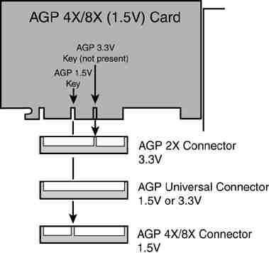
As you can see from Figure 15,
AGP 4X or 8X (1.5V) cards fit only in 1.5V or universal (3.3V or 1.5V) slots.
Due to the design of the connector and card keys, a 1.5V card cannot be
inserted into a 3.3V slot. So, if your new AGP card won't fit in the AGP slot
in your existing motherboard, consider that a good thing because if you were
able to plug it in, you would fry both the card and possibly the board as well!
In that case, you'd either have to return the 4X/8X card or get a new
motherboard that supports the 4X/8X (1.5V) cards.
Additionally, a newer
specification was introduced as AGP Pro 1.0 in August 1998 and was revised in
April 1999 as AGP Pro 1.1a. It defines a slightly longer slot with additional
power pins at each end to drive bigger and faster AGP cards that consume more than
25 watts of power, up to a maximum of 110 watts. AGP Pro cards are likely to be
used for high-end graphics workstations and are not likely to be found in any
normal PCs. However, AGP Pro slots are backward-compatible, meaning a standard
AGP card will plug in, and a number of motherboard vendors are using AGP Pro
slots rather than AGP 4x slots in their latest products. Because AGP Pro slots
are longer, an AGP 1x/2x card can be incorrectly inserted into the slot, which
could damage it, so some vendors supply a cover for the AGP Pro extension at
the rear of the slot. This cover should be removed only if you want to install
an AGP Pro card.
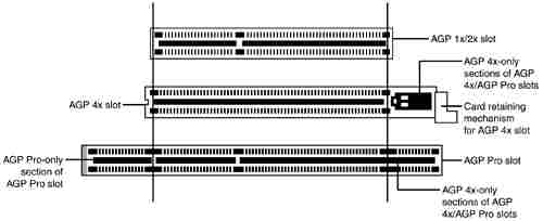
The standard AGP 1x/2x, AGP
4x, and AGP Pro slots are compared to each other in Figure 16.
The latest revision for the
AGP specification for PCs is AGP 8x, otherwise called AGP 3.0. AGP 8x defines a
transfer speed of 2,133MBps, which is twice that of AGP 4x. The AGP 8x
specification was first publicly pre-announced in November 2000. AGP 8x support
is now widely available in the latest motherboard chipsets and graphics
chipsets from major vendors. Although AGP 8x has a maximum speed twice that of
AGP 4x, the real-world differences between AGP 4x- and 8x-compatible devices
with otherwise identical specifications are minimal. However, many 3D chipsets that support AGP 8x are also upgrading memory and 3D
graphics core speeds and designs to better support the faster interface.
AGP is a high-speed connection
and runs at a base frequency of 66MHz (actually 66.66MHz), which is double that
of standard PCI. In the basic AGP mode, called 1x, a single transfer is done
every cycle. Because the AGP bus is 32 bits (4 bytes) wide, at 66 million times
per second it would be capable of transferring data at a rate of about 266MBps!
The original AGP specification also defines a 2x mode, in which two transfers
are performed every cycle, resulting in 533MBps. Using an analogy in which
every cycle is equivalent to the back-and-forth swing of a pendulum, the 1x mode
is thought of as transferring information at the start of each swing. In 2x
mode, an additional transfer would occur every time the pendulum completed half
a swing, thereby doubling performance while technically maintaining the same
clock rate, or in this case, the same number of swings per second. Although the
earliest AGP cards supported only the AGP 1x mode, most vendors quickly shifted
to the AGP 2x mode. The newer AGP 2.0 specification adds the capability for 4x
transfers, in which data is transferred four times per cycle and equals a data
transfer rate of 1,066MBps. Most newer AGP cards now have support for the 4x
standard as a minimum, and the latest graphics chipsets from NVIDIA and ATI
support AGP 8x. Table shows the differences in clock rates
and data transfer speeds (bandwidth) for the various AGP modes.
Because AGP is independent of
PCI, using an AGP video card frees up the PCI bus for more traditional input
and output, such as for IDE/ATA or SCSI controllers, USB controllers, sound
cards, and so on.
Besides faster video
performance, one of the main reasons Intel designed AGP was to allow the video
card to have a high-speed connection directly to the system RAM, which would
enable a reasonably fast and powerful video solution to be integrated at a
lower cost. AGP allows a video card to have direct access to the system RAM,
either enabling lower-cost video solutions to be directly built in to a
motherboard without having to include additional video RAM or enabling an AGP
card to share the main system memory. High-performance cards will likely
continue the trend of having more and more memory directly on the video card,
which is especially important when running high-performance 3D video
applications.
AGP allows the speed of the
video card to pace the requirements for high-speed 3D graphics rendering as
well as full motion video on the PC.