Processor Specifications
Many confusing specifications
often are quoted in discussions of processors. The following sections discuss
some of these specifications, including the data bus, address bus, and speed. The
next section includes a table that lists the specifications of virtually all PC
processors.
Processors can be identified
by two main parameters: how wide they are and how fast they are. The speed of a
processor is a fairly simple concept. Speed is counted in megahertz (MHz) and
gigahertz (GHz), which means millions and billions, respectively, of cycles per
second—and faster is better! The width of a processor is a little more
complicated to discuss because three main specifications in a processor are expressed
in width. They are
·
Data I/O bus
·
Address bus
·
Internal
registers
Note that the processor data
bus is also called the front side bus (FSB), processor side bus (PSB), or just
CPU bus. All these terms refer to the bus that is between the CPU and the main
chipset component (
The number of bits a processor
is designated can be confusing. All modern processors have 64-bit data buses;
however, that does not mean they are classified as 64-bit processors.
Processors such as the Pentium 4 and Athlon XP are
32-bit processors because their internal registers are 32 bits wide, although
their data I/O buses are 64 bits wide and their address buses are 36 bits wide
(both wider than their predecessors, the Pentium and K6 processors). The
Itanium series and the AMD Opteron and Athlon 64 are 64-bit processors because their internal
registers are 64 bits wide.
Data I/O Bus
Perhaps the most important
features of a processor are the speed and width of its external data bus. This
defines the rate at which data can be moved into or out of the processor.
The processor bus discussed
most often is the external data bus—the bundle of wires (or pins) used to send
and receive data. The more signals that can be sent at the same time, the more
data can be transmitted in a specified interval and, therefore, the faster (and
wider) the bus. A wider data bus is like having a highway with more lanes,
which enables greater throughput.
Data in a computer is sent as
digital information consisting of a time interval in which a single wire
carries 3.3V or 5V to signal a 1 data bit or 0V to signal a 0 data bit. The
more wires you have, the more individual bits you can send in the same time
interval. All modern processors from the original Pentium through the latest Pentium
4, Athlon XP, Athlon 64,
and even the Itanium and Itanium 2 have a 64-bit (8-byte) wide data bus.
Therefore, they can transfer 64 bits of data at a time to and from the
motherboard chipset or system memory.
A good way to understand this
flow of information is to consider a highway and the traffic it carries. If a
highway has only one lane for each direction of travel, only one car at a time
can move in a certain direction. If you want to increase traffic flow, you can
add another lane so that twice as many cars pass in a specified time. You can
think of an 8-bit chip as being a single-lane highway because 1 byte flows
through at a time. (1 byte equals 8 individual bits.) The 16-bit chip, with 2
bytes flowing at a time, resembles a two-lane highway. You might have four
lanes in each direction to move a large number of automobiles; this structure
corresponds to a 32-bit data bus, which has the capability to move 4 bytes of
information at a time. Taking this further, a 64-bit data bus is like having an
8-lane highway moving data in and out of the chip.
Another ramification of the
data bus in a chip is that the width of the data bus also defines the size of a
bank of memory. So, a processor with a 32-bit data bus such as the 486, reads and
writes memory 32 bits at a time. Pentium-class processors, including the
Pentium III, Celeron, Pentium 4, and Athlon XP, read
and write memory 64 bits at a time. 64-bit processors such as the Athlon 64 and Itanium series also read and write memory 64
bits at a time.
In 486 class systems, because
standard 72-pin single inline memory modules (SIMMs) are only 32 bits wide,
they must be installed one at a time in most 486 class systems. When used in
64-bit Pentium class systems, they must be installed two at a time. The current
module standard, dual inline memory modules (DIMMs),
are 64 bits wide. So, they are normally installed one at a time in Pentium or
newer systems. Each DIMM is equal to a complete bank of memory on a 64-bit data
bus, which makes system configuration easy because they can then be installed
or removed one at a time.
Starting in 2003 and beyond,
these classic rules for adding DIMM memory will begin to change, as
dual-channel chipsets such as the Intel 865 and 875 for the Pentium 4/Celeron 4
and the first Athlon 64 chipsets are introduced. To
improve memory performance, these and most, if not all, future chipsets will
support and eventually require that DIMM memory modules be installed in
identical pairs.
The Rambus
inline memory modules (RIMMs) used in some Pentium
III and 4 systems are somewhat of an anomaly because they play by a different
set of rules. They are typically only 16 or 32 bits wide. Depending on the
module type and chipset, they are either used individually or in pairs.
Address Bus
The address bus is the set of
wires that carries the addressing information used to describe the memory
location to which the data is being sent or from which the data is being
retrieved. As with the data bus, each wire in an address bus carries a single
bit of information. This single bit is a single digit in the address. The more
wires (digits) used in calculating these addresses, the greater the total
number of address locations. The size (or width) of the address bus indicates
the maximum amount of RAM a chip can address.
The highway analogy in the
"Data I/O Bus" section can be used to show how the address bus fits
in. If the data bus is the highway and the size of the data bus is equivalent
to the number of lanes, the address bus relates to the house number or street
address. The size of the address bus is equivalent to the number of digits in
the house address number. For example, if you live on a street in which the
address is limited to a two-digit (base 10) number, no more than 100 distinct
addresses (00–99) can exist for that street (102). Add another
digit, and the number of available addresses increases to 1,000 (000–999), or
103.
Computers use the binary (base
2) numbering system, so a two-digit number provides only four unique addresses
(00, 01, 10, and 11), calculated as 22. A three-digit number
provides only eight addresses (000–111), which is 23. For example,
the 8086 and 8088 processors use a 20-bit address bus that calculates as a
maximum of 220 or 1,048,576 bytes (1MB) of address locations. Table describes
the memory-addressing capabilities of processors.
Table . Processor Memory-Addressing Capabilities
|
||||||
|
Processor
Family |
Address
Bus |
Bytes |
Kilobytes
(KB) |
Megabytes
(MB) |
Gigabytes
(GB) |
Terabytes
(TB) |
|
8088/8086 |
20-bit |
1,048,576 |
1,024 |
1 |
— |
— |
|
286/386SX |
24-bit |
16,777,216 |
16,384 |
16 |
— |
— |
|
386DX/486/Pentium/K6 |
32-bit |
4,294,967,296 |
4,194,304 |
4,096 |
4 |
— |
|
Pentium Pro, Pentium II,
Pentium III, Celeron, Pentium 4, Athlon, Duron, Athlon 64 |
36-bit |
68,719,476,736 |
67,108,864 |
65,536 |
64 |
— |
|
Opteron |
40-bit |
1,099,511,627,776 |
1,073,741,824 |
1,048,576 |
1024 |
1 |
|
Itanium |
44-bit |
17,592,186,044,416 |
17,179,869,184 |
16,777,216 |
16,384 |
16 |
The data bus and address bus
are independent, and chip designers can use whatever size they want for each. Usually,
however, chips with larger data buses have larger address buses. The sizes of
the buses can provide important information about a chip's relative power,
measured in two important ways. The size of the data bus is an indication of
the chip's information-moving capability, and the size of the address bus tells
you how much memory the chip can handle.
Internal Registers
(Internal Data Bus)
The size of the internal
registers indicates how much information the processor can operate on at one
time and how it moves data around internally within the chip. This is sometimes
also referred to as the internal data bus. A register
is a holding cell within the processor; for example, the processor can add
numbers in two different registers, storing the result in a third register. The
register size determines the size of data on which the processor can operate.
The register size also describes the type of software or commands and
instructions a chip can run. That is, processors with 32-bit internal registers
can run 32-bit instructions that are processing 32-bit chunks of data, but
processors with 16-bit registers can't. Most advanced processors today—chips
from the 386 to the Pentium 4—use 32-bit internal registers and can therefore
run the same 32-bit operating systems and software. The Itanium and Athlon 64 processors have 64-bit internal registers, which
require new operating systems and software to fully be utilized.
Some very old processors have
an internal data bus (made up of data paths and storage units called registers)
that is larger than the external data bus. The 8088 and 386SX are examples of
this structure. Each chip has an internal data bus twice the width of the
external bus. These designs, which sometimes are called hybrid designs, usually are low-cost versions of a
"pure" chip. The 386SX, for example, can pass data around internally
with a full 32-bit register size; for communications with the outside world,
however, the chip is restricted to a 16-bit-wide data path. This design enabled
a systems designer to build a lower-cost motherboard with a 16-bit bus design
and still maintain software and instruction set compatibility with the full 32-bit
386. However, both the 8088 and the 386SX had lower performance than the 8086
and 386DX processors at the same speeds.
Internal registers often are
larger than the data bus, which means the chip requires two cycles to fill a
register before the register can be operated on. For example, both the 386SX
and 386DX have internal 32-bit registers, but the 386SX must "inhale"
twice (figuratively) to fill them, whereas the 386DX can do the job in one
"breath." The same thing would happen when the data is passed from
the registers back out to the system bus.
The Pentium is an example of
this type of design. All Pentiums have a 64-bit data bus and 32-bit registers—a
structure that might seem to be a problem until you understand that the Pentium
has two internal 32-bit pipelines for processing information. In many ways, the
Pentium is like two 32-bit chips in one. The 64-bit data bus provides for very
efficient filling of these multiple registers. Multiple pipelines are called superscalar architecture, which was introduced with
the Pentium processor.
More advanced sixth-generation
processors, such as the Pentium III, Athlon XP, and
Pentium 4, have as many as six internal pipelines for executing instructions.
Although some of these internal pipes are dedicated to special functions, these
processors can execute as many as six (Pentium 4) or nine (Athlon
XP) operations in one clock cycle.
Processor Modes
All Intel and Intel-compatible
32-bit processors (from the 386 on up) can run in several modes. Processor
modes refer to the various operating environments and affect the instructions
and capabilities of the chip. The processor mode controls how the processor
sees and manages the system memory and the tasks that use it.
The three modes of possible
operation are as follows:
·
Real mode
(16-bit software)
·
Protected mode
(32-bit software)
·
Virtual real
mode (16-bit programs within a 32-bit environment)
Real Mode
The original IBM PC included
an 8088 processor that could execute 16-bit instructions using 16-bit internal
registers and could address only 1MB of memory using 20 address lines. All
original PC software was created to work with this chip and was designed around
the 16-bit instruction set and 1MB memory model. For example, DOS and all DOS
software, Windows 1.x through 3.x, and all Windows 1.x through 3.x applications
are written using 16-bit instructions. These 16-bit operating systems and
applications are designed to run on an original 8088 processor.
Later processors such as the
286 could also run the same 16-bit instructions as the original 8088, but much
faster. In other words, the 286 was fully compatible with the original 8088 and
could run all 16-bit software just the same as an 8088, but, of course, that
software would run faster. The 16-bit instruction mode of the 8088 and 286
processors has become known as real mode. All software running in real
mode must use only 16-bit instructions and live within the 20-bit (1MB) memory
architecture it supports. Software of this type is usually single-tasking—only
one program can run at a time. No built-in protection exists to keep one
program from overwriting another program or even the operating system in
memory, so if more than one program is running, one of them could bring the
entire system to a crashing halt.
Protected (32-Bit)
Mode
Then came the 386, which was
the PC industry's first 32-bit processor. This chip could run an entirely new
32-bit instruction set. To take full advantage of the 32-bit instruction set, a
32-bit operating system and a 32-bit application were required. This new 32-bit
mode was referred to as protected mode, which alludes to the fact that
software programs running in that mode are protected from overwriting one
another in memory. Such protection helps make the system much more crash-proof
because an errant program can't very easily damage other programs or the
operating system. In addition, a crashed program can be terminated while the
rest of the system continues to run unaffected.
Knowing that new operating
systems and applications—which take advantage of the 32-bit protected
mode—would take some time to develop, Intel wisely built a backward-compatible
real mode into the 386. That enabled it to run unmodified 16-bit operating
systems and applications. It ran them quite well—much more quickly than any
previous chip. For most people, that was enough. They did not necessarily want
any new 32-bit software; they just wanted their existing 16-bit software to run
more quickly. Unfortunately, that meant the chip was never running in the
32-bit protected mode, and all the features of that capability were being
ignored.
When a high-powered processor
such as a Pentium 4 is running DOS (real mode), it acts like a "Turbo
8088." Turbo 8088 means the processor has the advantage of speed in
running any 16-bit programs; it otherwise can use only the 16-bit instructions
and access memory within the same 1MB memory map of the original 8088. Therefore,
if you have a 256MB Pentium 4 or Athlon system
running Windows 3.x or DOS, you are effectively using only the first megabyte
of memory, leaving the other 255MB largely unused!
New operating systems and
applications that ran in the 32-bit protected mode of the modern processors
were needed. Being stubborn, we resisted all the initial attempts at getting
switched over to a 32-bit environment. It seems that as a user community, we
are very resistant to change and would be content with our older software
running faster rather than adopting new software with new features. I'll be the
first one to admit that I was one of those stubborn users myself!
Because of this resistance,
true 32-bit operating systems such as Unix or variants (such as Linux), OS/2,
and even Windows NT/2000 or XP have taken a long time in getting a mainstream
share in the PC marketplace. Windows XP is the first full 32-bit OS that has
become a true mainstream product, and that is primarily because Microsoft has
coerced us in that direction with Windows 95, 98, and Me (which are mixed
16-/32-bit systems). Windows 3.x was the last full 16-bit operating system. In
fact, it was not really considered a complete operating system because it ran
on top of DOS.
The Itanium processor family
and the AMD Opteron add 64-bit native capability to
the table for servers, whereas the AMD Athlon 64
provides this capability for desktop computers. Both processors run all the
existing 32-bit software, but to fully take advantage of the processor, a
64-bit OS and applications are required. Microsoft has released 64-bit versions
of Windows XP, and several companies have released 64-bit applications for
networking and workstation use.
Note
The Intel Itanium family and
the AMD Athlon 64/Opteron use different 64-bit architectures.
Thus, 64-bit software written for one will not work on the other without being
recompiled by the software vendor. This means that software written
specifically for the Intel 64-bit architecture will not run on the AMD 64-bit
processors and vice versa.
Virtual Real Mode
The key to the backward
compatibility of the Windows 32-bit environment is the third mode in the
processor: virtual real mode. Virtual real is
essentially a virtual real mode 16-bit environment that runs inside 32-bit protected
mode. When you run a DOS prompt window inside Windows, you have created a
virtual real mode session. Because protected mode enables true multitasking,
you can actually have several real mode sessions running, each with its own
software running on a virtual PC. These can all run simultaneously, even while
other 32-bit applications are running.
Note that any program running
in a virtual real mode window can access up to only 1MB of memory, which that
program will believe is the first and only megabyte of memory in the system. In
other words, if you run a DOS application in a virtual real window, it will
have a 640KB limitation on memory usage. That is because there is only 1MB of
total RAM in a 16-bit environment and the upper 384KB is reserved for system
use. The virtual real window fully emulates an 8088 environment, so that aside
from speed, the software runs as if it were on an original real mode-only PC.
Each virtual machine gets its own 1MB address space, an image of the real
hardware BIOS routines, and emulation of all other registers and features found
in real mode.
Virtual real mode is used when
you use a DOS window to run a DOS or Windows 3.x 16-bit program. When you start
a DOS application, Windows creates a virtual DOS machine under which it can
run.
One interesting thing to note
is that all Intel and Intel-compatible (such as AMD and Cyrix) processors power
up in real mode. If you load a 32-bit operating system, it automatically
switches the processor into 32-bit mode and takes control from there.
It's also important to note
that some 16-bit (DOS and Windows 3.x) applications misbehave in a 32-bit
environment, which means they do things that even virtual real mode does not
support. Diagnostics software is a perfect example of this. Such software does
not run properly in a real-mode (virtual real) window under Windows. In that
case, you can still run your Pentium 4 in the original no-frills real mode by
either booting to a DOS floppy or, in the case of Windows 9x (excluding Me),
interrupting the boot process and commanding the system to boot plain DOS. This
is accomplished on Windows 9x systems by pressing the F8 key when you see the
prompt Starting Windows... on the screen or immediately after the beep when the
power on self test (POST) is completed. In the latter case, it helps to press
the F8 key multiple times because getting the timing just right is difficult
and Windows 9x looks for the key only during a short two-second time window.
If successful, you will then
see the Startup menu. You can select one of the command prompt choices that
tell the system to boot plain 16-bit real mode DOS. The choice of Safe Mode
Command Prompt is best if you are going to run true hardware diagnostics, which
do not normally run in protected mode and should be run with a minimum of
drivers and other software loaded.
Note that even though Windows
Me is based on Windows 98, Microsoft removed the Startup menu option in an
attempt to further wean us from any 16-bit operation. Windows NT, 2000, and XP
also lack the capability to interrupt the startup in this manner. For these
operating systems, you need a Startup Disk (floppy), which you can create and
then use to boot the system in real mode. Generally, you would do this to
perform certain maintenance procedures, such as running hardware diagnostics or
doing direct disk sector editing.
Although real mode is used by
16-bit DOS and "standard" DOS applications, special programs are
available that "extend" DOS and allow access to extended memory (over
1MB). These are sometimes called DOS extenders and usually are included as part of any DOS
or Windows 3.x software that uses them. The protocol that describes how to make
DOS work in protected mode is called DOS protected mode interface (DPMI).
DPMI was used by Windows 3.x to
access extended memory for use with Windows 3.x applications. It allowed these
programs to use more memory even though they were still 16-bit programs. DOS
extenders are especially popular in DOS games because they enable them to
access much more of the system memory than the standard 1MB most real mode
programs can address. These DOS extenders work by switching the processor in
and out of real mode. In the case of those that run under Windows, they use the
DPMI interface built into Windows, enabling them to share a portion of the
system's extended memory.
Another exception in real mode
is that the first 64KB of extended memory is actually accessible to the PC in
real mode, despite the fact that it's not supposed to be possible. This is the
result of a bug in the original IBM AT with respect to the 21st memory address
line, known as A20 (A0 is the first address line). By manipulating the A20
line, real-mode software can gain access to the first 64KB of extended
memory—the first 64KB of memory past the first megabyte. This area of memory is
called the high memory area (HMA).
Processor Speed
Ratings
A common misunderstanding
about processors is their different speed ratings. This section covers
processor speed in general and then provides more specific information about
Intel, AMD, and VIA/Cyrix processors.
A computer system's clock
speed is measured as a frequency, usually expressed as a number of cycles per
second. A crystal oscillator controls clock speeds using a sliver of quartz
sometimes contained in what looks like a small tin container. Newer systems
include the oscillator circuitry in the motherboard chipset, so it might not be
a visible separate component on newer boards. As voltage is applied to the
quartz, it begins to vibrate (oscillate) at a harmonic rate dictated by the
shape and size of the crystal (sliver). The oscillations emanate from the
crystal in the form of a current that alternates at the harmonic rate of the
crystal. This alternating current is the clock signal that forms the time base on
which the computer operates. A typical computer system runs millions of these
cycles per second, so speed is measured in megahertz. (One hertz is equal to
one cycle per second.) An alternating current signal is like a sine wave, with
the time between the peaks of each wave defining the frequency (see Figure).
Figure . Alternating current signal showing
clock cycle timing.
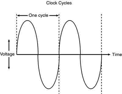
A single
cycle is the smallest element of time for the processor. Every action requires
at least one cycle and usually multiple cycles. To transfer data to and from
memory, for example, a modern processor such as the Pentium 4 needs a minimum
of three cycles to set up the first memory transfer and then only a single
cycle per transfer for the next
The time required to execute
instructions also varies:
·
8086 and 8088. The
original 8086 and 8088 processors take an average of 12 cycles to execute a
single instruction.
·
286 and 386. The 286 and
386 processors improve this rate to about 4.5 cycles per instruction.
·
486. The 486 and most
other fourth-generation Intel-compatible processors, such as the AMD 5x86, drop
the rate further, to about 2 cycles per instruction.
·
Pentium, K6 series. The
Pentium architecture and other fifth-generation Intel-compatible processors,
such as those from AMD and Cyrix, include twin instruction pipelines and other
improvements that provide for operation at one or two instructions per cycle.
·
Pentium Pro, Pentium II/III/4/Celeron, and Athlon/Athlon
XP/Duron.
These P6 and P7 (sixth- and seventh-generation) processors can execute as many
as three or more instructions per cycle.
Different instruction
execution times (in cycles) make comparing systems based purely on clock speed
or number of cycles per second difficult. How can two processors that run at
the same clock rate perform differently with one running "faster"
than the other? The answer is simple: efficiency.
The main reason the 486 was
considered fast relative to a 386 is that it executes twice as many
instructions in the same number of cycles. The same thing is true for a
Pentium; it executes about twice as many instructions in a given number of
cycles as a 486. Therefore, given the same clock speed, a Pentium is twice as
fast as a 486, and consequently a 133MHz 486 class processor (such as the AMD
5x86-133) is not even as fast as a 75MHz Pentium! That is because Pentium
megahertz are "worth" about double what 486 megahertz are worth in
terms of instructions completed per cycle. The Pentium II and III are about 50%
faster than an equivalent Pentium at a given clock speed because they can
execute about that many more instructions in the same number of cycles.
Comparing relative processor
performance, you can see that a 1GHz Pentium III is about equal to a
(theoretical) 1.5GHz Pentium, which is about equal to a 3GHz 486, which is
about equal to a 6GHz 386 or 286, which is about equal to a 12GHz 8088. The
original PC's 8088 ran at only 4.77MHz; today, we have systems that are
comparatively at least 2,500 times faster! As you can see, you must be careful
in comparing systems based on pure MHz alone because many other factors affect
system performance.
Overclocking
In some systems, the processor
speed can be set higher than the rating on the chip; this is called overclocking the chip. In many cases, you can get
away with a certain amount of overclocking because
Intel, AMD, and others often build safety margins into their ratings. So, a chip
rated for, say, 800MHz might in fact run at 900MHz or more but instead be
down-rated to allow for a greater margin of reliability. By overclocking,
you are using this margin and running the chip closer to its true maximum
speed. I don't normally recommend overclocking for a
novice, but if you are comfortable playing with your system settings, and you
can afford and are capable of dealing with any potential consequences, overclocking might enable you to get 10%–20% or more
performance from your system.
Overclocking Pitfalls
If you are intent on overclocking, there are several issues to consider. One is
that most Intel processors since the Pentium II are multiplier-locked before
they are shipped out. Therefore, the chip ignores any changes to the multiplier
setting on the motherboard. Actually, both Intel and AMD lock the multipliers
on most of their newer processors, but the AMD processors use solder bridges on
top of the chip that can be manipulated if you are careful and somewhat
mechanically inclined. Although originally done to prevent re-markers from
fraudulently relabeling processors (creating
"counterfeit" chips), this has impacted the computing performance
enthusiast, leaving tweaking the motherboard bus speed as the only easy way (or
in some cases, the only way possible) to achieve a clock speed higher than
standard.
You can run into problems
increasing motherboard bus speed, as well. Most Intel motherboards, for
example, simply don't support clock speeds other than the standard 66MHz,
100MHz, 133MHz, 400MHz, and 533MHz settings; the Intel D845PEBT2 motherboard,
introduced in late 2002, is an exception. Also all the Intel boards with speed
settings done via software (BIOS Setup), with the exception of the D845PEBT2
motherboard, read the proper settings from the installed processor and allow
only those settings. In other words, you simply plug in the processor, and the
Intel motherboard won't allow any settings other than what that processor is
designed for. Fortunately, most other brands do allow changing the bus speeds.
Even if
you could trick the processor into accepting a different clock multiplier
setting, the jump from 66MHz to 100MHz or from 100 to 133MHz is a large one, and many processors will not make that much of a jump
reliably. For example, a Pentium III 800E runs at a 100MHz bus speed with an 8x
multiplier. Bumping the motherboard speed to 133MHz causes the processor to try
to run at 8x133, or 1066MHz. It is not certain that the chip would run reliably
at that speed. Likewise, a Celeron 600E runs at 9x66MHz. Raising the bus speed
to 100MHz causes the chip to try and run at 9x100MHz, or 900MHz, another
potentially unsuccessful change.
A board that supports
intermediate speed settings and allows the settings to be changed in smaller
increments is necessary. This is because a given chip is generally overclockable by a certain percentage. The smaller the
steps you can take when increasing speed, the more likely that you'll be able
to come close to the actual maximum speed of the chip without going over. For
example, the Asus P3V4X motherboard supports front-side bus speed settings of
66MHz, 75MHz, 83MHz, 90MHz, 95MHz, 100MHz, 103MHz, 105MHz, 110MHz, 112MHz,
115MHz, 120MHz, 124MHz, 133MHz, 140MHz, and 150MHz. By setting the 800MHz
Pentium IIIE to increments above 100MHz, you'd have the following:
|
Multiplier
(Fixed) |
Bus
Speed |
Processor
Speed |
|
8x |
100MHz |
800MHz |
|
8x |
103MHz |
824MHz |
|
8x |
105MHz |
840MHz |
|
8x |
110MHz |
880MHz |
|
8x |
112MHz |
896MHz |
|
8x |
115MHz |
920MHz |
|
8x |
120MHz |
960MHz |
|
8x |
124MHz |
992MHz |
|
8x |
133MHz |
1066MHz |
Likewise, using this
motherboard with a Celeron 600, you could try settings above the standard 66MHz
bus speed as follows:
|
Multiplier
(Fixed) |
Bus
Speed |
Processor
Speed |
|
9x |
66MHz |
600MHz |
|
9x |
75MHz |
675MHz |
|
9x |
83MHz |
747MHz |
|
9x |
90MHz |
810MHz |
|
9x |
95MHz |
855MHz |
|
9x |
100MHz |
900MHz |
Typically, a 10%–20% increase
is successful, so with this motherboard, you are likely to get your processor
running 100MHz or faster than it was originally designed for.
An issue when it comes to
increasing CPU bus speeds is that the other buses in the system will typically
be similarly affected. Thus, if you increase the CPU bus speed by 10%, you might
also be increasing the PCI or AGP bus by the same amount, and your video,
network, or other cards might not be able to keep up. This is something that
varies from board to board, so you have to consider each example as a
potentially unique case.
Overclocking Socket A Processors
The AMD Athlon
and Duron processors in the FC-PGA (flip-chip pin
grid array) format, which plugs into Socket A, have special solder bridges on
the top face of the chip that can be modified to change or remove the lock from
the internal multiplier on the chip. This can increase the speed of the chip
without changing the motherboard bus speed, thus affecting other buses or
cards.
The selected multiplier is set
or locked by very small solder connections between solder dots (contacts) on
the surface of the chip. You can completely unlock the chip by bridging or
disconnecting the appropriate dots. Unfortunately, it is somewhat difficult to
add or remove these bridges; you usually have to mask off the particular bridge
you want to create and, rather than dripping solder onto it, literally paint
the bridge with silver or copper paint. For example, you can use the special
copper paint sold in small vials at any auto parts store for repairing the
window defogger grids. The real problem is that the contacts are very small,
and if you bridge to adjacent rather than opposite contacts, you can render the
chip nonfunctional. An exacto knife or razor blade
can be used to remove the bridges if desired. If you are not careful, you can
easily damage a processor worth several hundred dollars. If you are leery of
making such changes, you should try bus overclocking
instead because this is done in the BIOS Setup and can easily be changed or
undone without any mechanical changes to the chip.
CPU Voltage Settings
Another trick used by overclockers is playing with the voltage settings for the
CPU. All modern CPU sockets and slots, including Slot 1, Slot A, Socket 8,
Socket 370, Socket 423, Socket 478, and Socket A, have automatic voltage
detection. With this detection, the system detects and sets the correct voltage
by reading certain pins on the processor. Some motherboards, such as those made
by Intel, do not allow any manual changes to these settings. Other
motherboards, such as the Asus P3V4X mentioned earlier, allow you to tweak the
voltage settings from the automatic setting up or down by tenths of a volt.
Some experimenters have found that by either increasing or decreasing voltage
slightly from the standard, a higher speed of overclock
can be achieved with the system remaining stable.
Cache Memory
As processor core speeds
increased, memory speeds could not keep up. How could you run a processor
faster than the memory from which you feed it without having performance suffer
terribly? The answer was cache. In its simplest terms, cache
memory is a high-speed memory buffer that temporarily stores data the
processor needs, allowing the processor to retrieve that data faster than if it
came from main memory. But there is one additional feature of a cache over a
simple buffer, and that is intelligence. A cache is a buffer with a brain.
A buffer holds random data,
usually on a first in, first out, or first in, last out basis. A cache, on the
other hand, holds the data the processor is most likely to need in advance of
it actually being needed. This enables the processor to continue working at
either full speed or close to it without having to wait for the data to be
retrieved from slower main memory. Cache memory is usually made up of static
RAM (SRAM) memory integrated into the processor die, although older systems
with cache also used chips installed on the motherboard.
Two levels of processor/memory
cache are used in a modern PC, called Level 1 (L1) and Level 2 (L2) (some
server processors such as the Itanium series from Intel also have Level 3
cache). These caches and how they function are described in the following
sections.
Internal Level 1
Cache
All modern processors starting
with the 486 family include an integrated L1 cache and controller. The
integrated L1 cache size varies from processor to processor, starting at 8KB
for the original 486DX and now up to 32KB, 64KB, or more in the latest
processors.
To understand the importance
of cache, you need to know the relative speeds of processors and memory. The
problem with this is that processor speed usually is expressed in MHz or GHz
(millions or billions of cycles per second), whereas memory speeds are often
expressed in nanoseconds (billionths of a second per cycle). Most newer types
of memory express the speed in either MHz or in megabyte per second (MBps) bandwidth (throughput).
Because L1 cache is always
built into the processor die, it runs at the full-core speed of the processor
internally. By full-core speed, I mean this cache runs at the higher clock
multiplied internal processor speed rather than the external motherboard speed.
This cache basically is an area of very fast memory built into the processor
and is used to hold some of the current working set of code and data. Cache
memory can be accessed with no wait states because it is running at the same
speed as the processor core.
Using cache memory reduces a
traditional system bottleneck because system RAM is almost always much slower
than the CPU; the performance difference between memory and CPU speed has
become especially large in recent systems. Using cache memory prevents the
processor from having to wait for code and data from much slower main memory,
therefore improving performance. Without the L1 cache, a processor would
frequently be forced to wait until system memory caught up.
Cache is even more important
in modern processors because it is often the only memory in the entire system
that can truly keep up with the chip. Most modern processors are clock
multiplied, which means they are running at a speed that is really a multiple
of the motherboard into which they are plugged. The Pentium 4 2.8GHz, for
example, runs at a multiple of 5.25 times the true motherboard speed of 533MHz.
The main memory is one half this speed (266MHz) because the Pentium 4 uses a
quad-pumped memory bus. Because the main memory is plugged into the
motherboard, it can run only at 266MHz maximum. The only 2.8GHz memory in such
a system is the L1 and L2 caches built into the processor core. In this
example, the Pentium 4 2.8GHz processor has 20KB of integrated L1 cache (8KB
data cache and 12KB execution trace cache) and 512KB of L2, all running at the
full speed of the processor core.
If the data the processor
wants is already in the internal cache, the CPU does not have to wait. If the
data is not in the cache, the CPU must fetch it from the Level 2 cache or (in
less sophisticated system designs) from the system bus, meaning main memory
directly.
How Cache Works
To learn how the L1 cache
works, consider the following analogy.
This story involves a person
(in this case you) eating food to act as the processor requesting and operating
on data from memory. The kitchen where the food is prepared is the main memory
(SIMM/DIMM) RAM. The cache controller is the waiter, and the L1 cache is the
table at which you are seated.
Okay, here's the story. Say
you start to eat at a particular restaurant every day at the same time. You
come in, sit down, and order a hot dog. To keep this story proportionately
accurate, let's say you normally eat at the rate of one bite (byte? <g>)
every four seconds (233MHz = about 4ns cycling). It also takes 60 seconds for
the kitchen to produce any given item that you order (60ns main memory).
So, when you first arrive, you
sit down, order a hot dog, and you have to wait for 60 seconds for the food to
be produced before you can begin eating. After the waiter brings the food, you
start eating at your normal rate. Pretty quickly you finish the hot dog, so you
call the waiter over and order a hamburger. Again you wait 60 seconds while the
hamburger is being produced. When it arrives, you again begin eating at full speed.
After you finish the hamburger, you order a plate of fries. Again you wait, and
after it is delivered 60 seconds later, you eat it at full speed. Finally, you
decide to finish the meal and order cheesecake for dessert. After another
60-second wait, you can eat cheesecake at full speed. Your overall eating
experience consists of mostly a lot of waiting, followed by short bursts of
actual eating at full speed.
After coming into the
restaurant for two consecutive nights at exactly
This analogy exactly describes
the function of the L1 cache in the processor. The L1 cache itself is the table
that can contain one or more plates of food. Without a waiter, the space on the
table is a simple food buffer. When stocked, you can eat until the buffer is
empty, but nobody seems to be intelligently refilling it. The waiter is the
cache controller who takes action and adds the intelligence to decide which
dishes are to be placed on the table in advance of your needing them. Like the
real cache controller, he uses his skills to literally guess which food you
will require next, and if and when he guesses right, you never have to wait.
Let's now say on the fourth
night you arrive exactly on time and start off with the usual hot dog. The
waiter, by now really feeling confident, has the hot dog already prepared when
you arrive, so there is no waiting.
Just as you finish the hot
dog, and right as he is placing a hamburger on your plate, you say "Gee,
I'd really like a bratwurst now; I didn't actually order this hamburger."
The waiter guessed wrong, and the consequence is that this time you have to
wait the full 60 seconds as the kitchen prepares your brat. This is known as a cache miss, in which the cache controller did not
correctly fill the cache with the data the processor actually needed next. The
result is waiting, or in the case of a sample 233MHz Pentium system, the system
essentially throttles back to 16MHz (RAM speed) whenever a cache miss occurs.
According to Intel, the L1
cache in most of its processors has approximately a 90% hit ratio (some
processors, such as the Pentium 4, are slightly higher). This means that the
cache has the correct data 90% of the time, and consequently the processor runs
at full speed—233MHz in this example—90% of the time. However, 10% of the time
the cache controller guesses wrong and the data has to be retrieved out of the
significantly slower main memory, meaning the processor has to wait. This
essentially throttles the system back to RAM speed, which in this example was
60ns or 16MHz.
In this analogy, the processor
was 14 times faster than the main memory. Memory speeds have increased from
16MHz (60ns) to 333MHz (3.0ns) or faster in the latest systems, but processor
speeds have also risen to 3GHz and beyond, so even in the latest systems,
memory is still 7.5 or more times SLOWER than the processor. Cache is what
makes up the difference.
The main feature of L1 cache
is that it has always been integrated into the processor core, where it runs at
the same speed as the core. This, combined with the hit ratio of 90% or
greater, makes L1 cache very important for system performance.
Level 2 Cache
To mitigate the dramatic
slowdown every time an L1 cache miss occurs, a secondary (L2) cache is
employed.
Using the restaurant analogy I
used to explain L1 cache in the previous section, I'll equate the L2 cache to a
cart of additional food items placed strategically in the restaurant such that
the waiter can retrieve food from the cart in only 15 seconds (versus 60
seconds from the kitchen). In an actual Pentium class (Socket 7) system, the L2
cache is mounted on the motherboard, which means it runs at motherboard speed—66MHz,
or 15ns in this example. Now, if you ask for an item the waiter did not bring
in advance to your table, instead of making the long trek back to the kitchen
to retrieve the food and bring it back to you 60 seconds later, he can first
check the cart where he has placed additional items. If the requested item is
there, he will return with it in only 15 seconds. The net effect in the real
system is that instead of slowing down from 233MHz to 16MHz waiting for the
data to come from the 60ns main memory, the data can instead be retrieved from
the 15ns (66MHz) L2 cache. The effect is that the system slows down from 233MHz
to 66MHz.
Newer processors have
integrated L2 cache that runs at the same speed as the processor core, which is
also the same speed as the L1 cache. For the analogy to describe these newer
chips, the waiter would simply place the cart right next to the table you were
seated at in the restaurant. Then, if the food you desired wasn't on the table
(L1 cache miss), it would merely take a longer reach over to the adjacent L2
cache (the cart, in this analogy) rather than a 15-second walk to the kitchen
as with the older designs.
Cache Performance
and Design
Just as with the L1 cache,
most L2 caches have a hit ratio also in the 90% range; therefore, if you look
at the system as a whole, 90% of the time it will be running at full speed
(233MHz in this example) by retrieving data out of the L1 cache. Ten percent of
the time it will slow down to retrieve the data from the L2 cache. Ninety
percent of the time the processor goes to the L2 cache, the data will be in the
L2, and 10% of that time it will have to go to the slow main memory to get the
data because of an L2 cache miss. So, by combining both caches, our sample
system runs at full processor speed 90% of the time (233MHz in this case), at
motherboard speed 9% (90% of 10%) of the time (66MHz in this case), and at RAM
speed about 1% (10% of 10%) of the time (16MHz in this case). You can clearly
see the importance of both the L1 and L2 caches; without them the system uses
main memory more often, which is significantly slower than the processor.
This brings up other
interesting points. If you could spend money doubling the performance of either
the main memory (RAM) or the L2 cache, which would you improve? Considering
that main memory is used directly only about 1% of the time, if you doubled
performance there, you would double the speed of your system only 1% of the
time! That doesn't sound like enough of an improvement to justify much expense.
On the other hand, if you doubled L2 cache performance, you would be doubling
system performance 9% of the time, a much greater improvement overall. I'd much
rather improve L2 than RAM performance.
The processor and system designers
at Intel and AMD know this and have devised methods of improving the
performance of L2 cache. In Pentium (P5) class systems, the L2 cache usually
was found on the motherboard and had to therefore run at motherboard speed.
Intel made the first dramatic improvement by migrating the L2 cache from the
motherboard directly into the processor and initially running it at the same
speed as the main processor. The cache chips were made by Intel and mounted
next to the main processor die in a single chip housing. This proved too
expensive, so with the Pentium II Intel began using cache chips from
third-party suppliers such as Sony, Toshiba, NEC, Samsung, and others. Because
these were supplied as complete packaged chips and not raw die, Intel mounted
them on a circuit board alongside the processor. This is why the Pentium II was
designed as a cartridge rather than what looked like a chip.
One problem was the speed of
the available third-party cache chips. The fastest ones on the market were 3ns
or higher, meaning 333MHz or less in speed. Because the processor was being
driven in speed above that, in the Pentium II and initial Pentium III
processors Intel had to run the L2 cache at half the processor speed because
that is all the commercially available cache memory could handle. AMD followed
suit with the Athlon processor, which had to drop L2
cache speed even further in some models to two-fifths or one-third the main CPU
speed to keep the cache memory speed less than the 333MHz commercially
available chips.
Then a breakthrough occurred,
which first appeared in Celeron processors 300A and above. These had 128KB of
L2 cache, but no external chips were used. Instead, the L2 cache had been
integrated directly into the processor core just like the L1. Consequently, both
the L1 and L2 caches now would run at full processor speed, and more
importantly scale up in speed as the processor speeds increased in the future.
In the newer Pentium III, as well as all the Xeon and Celeron processors, the
L2 cache runs at full processor core speed, which means there is no waiting or
slowing down after an L1 cache miss. AMD also achieved full-core speed on-die
cache in its later Athlon and Duron
chips. Using on-die cache improves performance dramatically because the 9% of
the time the system would be using the L2 it would now remain at full speed
instead of slowing down to one-half or less the processor speed or, even worse,
slow down to motherboard speed as in Socket 7 designs. Another benefit of
on-die L2 cache is cost, which is less because now fewer parts are involved.
Let's revisit the restaurant
analogy using a modern Pentium 4 2GHz. You would now be taking a bite every
half second (2GHz = 0.5ns cycling). The L1 cache would also be running at that
speed, so you could eat anything on your table at that same rate (the table =
L1 cache). The real jump in speed comes when you want something that isn't
already on the table (L1 cache miss), in which case the waiter reaches over to
the cart (which is now directly adjacent to the table) and nine out of ten
times is able to find the food you want in only one-half second (L2 speed =
2GHz or 0.5ns cycling). In this more modern system, you would run at 2GHz 99%
of the time (L1 and L2 hit ratios combined) and slow down to RAM speed (wait
for the kitchen) only 1% of the time as before.
With faster memory running at
400MHz (2.5ns), you would have to wait only 2.5 seconds for the food to come
from the kitchen. If only restaurant performance would increase at the same
rate processor performance has!
Cache Organization
You know that cache stores
copies of data from various main memory addresses. Because the cache cannot
hold copies of the data from all the addresses in main memory simultaneously,
there has to be a way to know which addresses are currently copied into the
cache so that, if we need data from those addresses, it can be read from the
cache rather than from the main memory. This function is performed by Tag RAM,
which is additional memory in the cache that holds an index of the addresses that
are copied into the cache. Each line of cache memory has a corresponding
address tag that stores the main memory address of the data currently copied
into that particular cache line. If data from a particular main memory address
is needed, the cache controller can quickly search the address tags to see
whether the requested address is currently being stored in the cache (a hit) or
not (a miss). If the data is there, it can be read from the faster cache; if it
isn't, it has to be read from the much slower main memory.
Various ways of organizing or
mapping the tags affect how cache works. A cache can be mapped as fully
associative, direct-mapped, or set associative.
In a fully associative mapped
cache, when a request is made for data from a specific main memory address, the
address is compared against all the address tag entries in the cache tag RAM.
If the requested main memory address is found in the tag (a hit), the corresponding location in the cache is
returned. If the requested address is not found in the address tag entries, a miss occurs and the data must be retrieved from the
main memory address instead of the cache.
In a direct-mapped cached,
specific main memory addresses are preassigned to
specific line locations in the cache where they will be stored. Therefore, the
tag RAM can use fewer bits because when you know which main memory address you
want, only one address tag needs to be checked and each tag needs to store only
the possible addresses a given line can contain. This also results in faster
operation because only one tag address needs to be checked for a given memory
address.
A set associative cache is a
modified direct-mapped cache. A direct-mapped cache has only one set of memory
associations, meaning a given memory address can be mapped into (or associated
with) only a specific given cache line location. A two-way set associative
cache has two sets, so that a given memory location can be in one of two
locations. A four-way set associative cache can store a given memory address
into four different cache line locations (or sets). By increasing the set associativity, the chance of finding a value increases;
however, it takes a little longer because more tag addresses must be checked
when searching for a specific location in the cache. In essence, each set in an
n-way set associative cache is a sub-cache that has associations with each main
memory address. As the number of sub-caches or sets increases, eventually the
cache becomes fully associative—a situation in which any memory address can be stored
in any cache line location. In that case, an n-way set associative cache is a
compromise between a fully associative cache and a direct-mapped cache.
In general, a direct-mapped
cache is the fastest at locating and retrieving data from the cache because it
has to look at only one specific tag address for a given memory address.
However, it also results in more misses overall than the other designs. A fully
associative cache offers the highest hit ratio but is the slowest at locating
and retriving the data because it has many more
address tags to check through. An n-way set associative cache is a compromise
between optimizing cache speed and hit ratio, but the more associativity
there is, the more hardware (tag bits, comparator circuits, and so on) is required,
making the cache more expensive. Obviously, cache design is a series of
tradeoffs, and what works best in one instance might not work best in another.
Multitasking environments such as Windows are good examples of environments in
which the processor needs to operate on different areas of memory
simultaneously and in which an n-way cache can improve performance.
The organization of the cache
memory in the 486 and MMX Pentium family is called a four-way
set associative cache, which means that the cache memory is split into
four blocks. Each block also is organized as 128 or 256 lines of 16 bytes each.
The following table shows the associativity of
various processor L1 and L2 caches.
|
Processor |
L1
Cache Associativity |
L2
Cache Associativity |
|
486 |
Four-way |
Not in CPU |
|
Pentium (non-MMX) |
Two-way |
Not in CPU |
|
Pentium MMX |
Four-way |
Not in CPU |
|
Pentium Pro/II/III |
Four-way |
Four-way (off-die) |
|
Pentium III/4 |
Four-way |
Eight-way (on-die) |
The contents of the cache must
always be in sync with the contents of main memory to ensure that the processor
is working with current data. For this reason, the internal cache in the 486
family is a write-through cache. Write-through
means that when the processor writes information out to the cache, that
information is automatically written through to main memory as well.
By comparison, the Pentium and
later chips have an internal write-back cache, which means that both reads and
writes are cached, further improving performance. Even though the internal 486
cache is write-through, the system can employ an external write-back cache for
increased performance. In addition, the 486 can buffer up to 4 bytes before
actually storing the data in RAM, improving efficiency in case the memory bus is
busy.
Another feature of improved
cache designs is that they are nonblocking. This is a
technique for reducing or hiding memory delays by exploiting the overlap of
processor operations with data accesses. A nonblocking cache enables program execution to proceed
concurrently with cache misses as long as certain dependency constraints are
observed. In other words, the cache can handle a cache miss much better and
enable the processor to continue doing something nondependent on the missing
data.
The cache controller built
into the processor also is responsible for watching the memory bus when
alternative processors, known as bus masters,
are in control of the system. This process of watching the bus is referred to
as bus snooping. If a bus master device writes
to an area of memory that also is stored in the processor cache currently, the
cache contents and memory no longer agree. The cache controller then marks this
data as invalid and reloads the cache during the next memory access, preserving
the integrity of the system.
All PC processor designs that
support cache memory include a feature known as a translation look aside buffer
(TLB) to improve recovery from cache misses. The TLB is a table inside the
processor that stores information about the location of recently accessed
memory addresses. The TLB speeds up the translation of virtual addresses to
physical memory addresses. To improve TLB performance, several recent
processors have increased the number of entries in the TLB, as AMD did when it
moved from the Athlon Thunderbird core to the
Palomino core. Pentium 4 processors that support HT Technology have a separate
instruction TLB (iTLB) for each virtual processor
thread.
As clock speeds increase,
cycle time decreases. Newer systems don't use cache on the motherboard any
longer because the faster DDR-SDRAM or RDRAM used in modern Pentium 4/Celeron
or Athlon systems can keep up with the motherboard speed. Modern processors all
integrate the L2 cache into the processor die just like the L1 cache. This
enables the L2 to run at full-core speed because it is now a part of the core.
Cache speed is always more important than size. The rule is that a smaller but
faster cache is always better than a slower but bigger cache. Table 3.10
illustrates the need for and function of L1 (internal) and L2 (external)
caches in modern systems.
Table 3.10. CPU Speeds Relative to Cache, RAM, and
Motherboard
|
||||
|
CPU Type |
Pentium |
Pentium
Pro |
Pentium
II |
AMD K6-2 |
|
CPU speed |
233MHz |
200MHz |
450MHz |
550MHz |
|
L1 cache speed |
4.3ns (233MHz) |
5.0ns (200MHz) |
2.2ns (450MHz) |
1.8ns (550MHz) |
|
L1 cache size |
16K |
32K |
32K |
64K |
|
L2 cache type |
onboard |
on-chip |
on-chip |
onboard |
|
L2 speed ratio |
— |
1/1 |
1/2 |
— |
|
L2 cache speed |
15ns (66MHz) |
5ns (200MHz) |
4.4ns (225MHz) |
10ns (100MHz) |
|
L2 cache size |
varies[1] |
256KB[2] |
512KB |
varies[1] |
|
CPU bus speed |
66MHz |
66MHz |
100MHz |
100MHz |
|
Memory bus speed |
60ns (16MHz) |
60ns (16MHz) |
10ns (100MHz) |
|
|
CPU Type |
AMD K6-3 |
Duron |
Athlon |
Athlon XP |
|
CPU speed |
450MHz |
1.3GHz |
1.4GHz |
2.167GHz |
|
L1 cache speed |
2.2ns (450MHz) |
0.77ns (1.3GHz) |
0.71ns (1.4GHz) |
0.46ns (2.167GHz) |
|
L1 cache size |
64K |
128K |
128K |
128K |
|
L2 cache type |
on-die |
on-die |
on-die |
on-die |
|
L2 speed ratio |
1/1 |
1/1 |
1/1 |
1/1 |
|
L2 cache speed |
2.2ns (450MHz) |
0.77ns (1.3GHz) |
0.71ns (1.4GHz) |
0.46ns (2.167GHz) |
|
L2 cache size |
256KB |
64KB |
256KB |
512KB |
|
CPU bus speed |
100MHz |
200MHz |
266MHz |
333MHz |
|
Memory bus speed |
10ns (100MHz) |
5ns (200MHz) |
3.8ns (266MHz) |
|
|
CPU Type |
Pentium
III |
Celeron/370 |
Celeron/478 |
Pentium
4 |
|
CPU speed |
1.4GHz |
1.4GHz |
2.2GHz |
2.53GHz |
|
L1 cache speed |
0.71ns (1.4GHz) |
0.71ns (1.4GHz) |
0.45ns (2.2GHz) |
0.39ns (2.53GHz) |
|
L1 cache size |
32K |
32K |
20K |
20K |
|
L2 cache type |
on-die |
on-die |
on-die |
on-die |
|
L2 speed ratio |
1/1 |
1/1 |
1/1 |
1/1 |
|
L2 cache speed |
0.71ns (1.4GHz) |
0.71ns (1.4GHz) |
0.45ns (2.2GHz) |
0.39ns (2.53GHz) |
|
L2 cache size |
512KB |
256KB |
128KB |
512KB |
|
CPU bus speed |
133MHz |
100MHz |
400MHz |
533MHz |
|
Memory bus speed |
7.5ns (133MHz) |
10ns (100MHz) |
2.5ns (400MHz)[3] |
1.9ns (533MHz)[3] |
|
4. This
example is based on the AMD Athlon XP 3000+,
which uses the Barton core. Palomino- and Thoroughbred-core versions of the Athlon XP have 256KB L2 caches. |
||||
[1] The L2 cache is on the motherboard, and the amount depends on
which board is chosen and how much is installed.
[2] The Pentium Pro was also available with 512KB and 1024KB L2
cache.
[3] Note RDRAM used on some
motherboards with these processors technically runs at 800MHz or 1066MHz, but
the RDRAM bus is only 32 bits wide, resulting in
a bandwidth of either 3.2GBps or 4.2GBps, which is equivalent in bandwidth to
running at 400MHz or 533MHz at the 64-bit width of the processor data bus. Some
motherboards for these processors use DDR266 or DDR333 memory instead, which
has a bandwidth of 2.1GBps or 2.7GBps.
As you can see, having two
levels of cache between the very fast CPU and the much slower main memory helps
minimize any wait states the processor might have to endure, especially those
with the on-die L2. This enables the processor to keep working closer to its
true speed.