Processor Socket and Slot Types
Intel and AMD have created a
set of socket and slot designs for their processors. Each socket or slot is
designed to support a different range of original and upgrade processors. Table
shows the specifications of these sockets.
Table.
CPU Socket and Slot Types and Specifications
|
|||||
|
Socket
Number |
Pins |
Pin
Layout |
Voltage |
Supported
Processors |
Introduced |
|
Socket 1 |
169 |
17x17 PGA |
5V |
486 SX/SX2, DX/DX2[1],
DX4 OverDrive |
April '89 |
|
Socket 2 |
238 |
19x19 PGA |
5V |
486 SX/SX2, DX/DX2[1],
DX4 OverDrive, 486 Pentium OverDrive |
March '92 |
|
Socket 3 |
237 |
19x19 PGA |
5V/3.3V |
486 SX/SX2, DX/DX2, DX4, 486
Pentium OverDrive, AMD 5x86 |
Feb. '94 |
|
Socket 4 |
273 |
21x21 PGA |
5V |
Pentium 60/66, OverDrive |
March '93 |
|
Socket 5 |
320 |
37x37 SPGA |
3.3/3.5V |
Pentium 75-133, OverDrive |
Oct. '94 |
|
Socket 62 |
235 |
19x19 PGA |
3.3V |
486 DX4, 486 Pentium OverDrive |
Feb. '94 |
|
Socket 7 |
321 |
37x37 SPGA |
VRM |
Pentium 75-233+, MMX, OverDrive, AMD K5/K6, Cyrix M1/II |
Jan. '97 |
|
Socket 8 |
387 |
DP-SPGA |
Auto VRM |
Pentium Pro, OverDrive |
Nov. '95 |
|
Socket 370 |
370 |
37x37 SPGA |
Auto VRM |
Celeron/Pentium III
PPGA/FC-PGA |
Aug. '98 |
|
Socket PAC418 |
418 |
38x22 S-SPGA |
Auto VRM |
Itanium |
May '01 |
|
Socket 423 |
423 |
39x39 SPGA |
Auto VRM |
Pentium 4 FC-PGA2 |
Nov. '00 |
|
Socket A (462) |
462 |
37x37 SPGA |
Auto VRM |
AMD Athlon/Duron
FC-PGA |
June '00 |
|
Socket 478 |
478 |
26x26 mPGA |
Auto VRM |
Pentium 4 FC-PGA2 |
Oct. '01 |
|
Socket 603 |
603 |
31x25 mPGA |
Auto VRM |
Xeon (P4) |
May '01 |
|
Socket 754 |
754 |
29x29 mPGA |
Auto VRM |
Athlon 64 |
Sep. '03 |
|
Socket 940 |
940 |
31x31 mPGA |
|
AMD Opteron |
April '03 |
|
Slot A |
242 |
Slot |
Auto VRM |
AMD Athlon
SECC |
June '99 |
|
Slot 1 (SC242) |
242 |
Slot |
Auto VRM |
Pentium II/III, Celeron SECC |
May '97 |
|
Slot 2 (SC330) |
330 |
Slot |
Auto VRM |
Pentium II/III Xeon SECC |
|
|
2. Socket
6 was a paper standard only and was never actually implemented in any
systems. DP-SPGA
= Dual-pattern staggered PGA FC-PGA = Flip-chip PGA FC-PGA2
= Second-generation flip-chip PGA mPGA = Micro PGA PAC
= Pin array cartridge PGA = Pin grid array PPGA
= Plastic PGA S-SPGA
= SECC
= Single edge contact cartridge SPGA
= Staggered PGA VRM
= Voltage regulator module |
|||||
[1] Non-overdrive DX4 or AMD 5x86
can also be supported with the addition of an aftermarket 3.3V
voltage-regulator adapter.
Sockets 1, 2, 3, and 6 are 486
processor sockets and are shown together in Figure 1 so you can see the overall
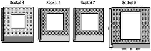
size comparisons and pin arrangements between these sockets. Sockets 4, 5, 7,
and 8 are Pentium and Pentium Pro processor sockets and are shown together in
Figure 2 so you can see the overall size comparisons and pin arrangements
between these sockets. More detailed drawings of each socket are included
throughout the remainder of this section with thorough descriptions of the
sockets.
Figure 1. 486 processor sockets.
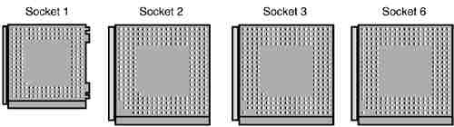
Figure 2. Pentium and Pentium Pro processor
sockets.
Zero Insertion
Force
When the Socket 1
specification was created, manufacturers realized that if users were going to
upgrade processors, they had to make the process easier. The socket
manufacturers found that 100 lbs. of insertion force is required to install a
chip in a standard 169-pin screw Socket 1 motherboard. With this much force
involved, you easily could damage either the chip or the socket during removal
or reinstallation. Because of this, some motherboard manufacturers began using
low insertion force (LIF) sockets, which required only 60 lbs. of insertion
force for a 169-pin chip. With the LIF or standard socket, I usually advise
removing the motherboard that way you can support the board from behind when
you insert the chip. Pressing down on the motherboard with 60-100 lbs. of force
can crack the board if it is not supported properly. A special tool is also
required to remove a chip from one of these sockets. As you can imagine, even
the low insertion force was relative, and a better solution was needed if the
average person was ever going to replace his CPU.
Manufacturers began using ZIF
sockets in Socket 1 designs, and all processor sockets
from Socket 2 and higher have been of the ZIF design. ZIF is required for all
the higher-density sockets because the insertion force would simply be too
great otherwise. ZIF sockets almost eliminate the risk involved in installing or
removing a processor because no insertion force is necessary to install the
chip and no tool is needed to extract one. Most ZIF sockets are
handle-actuated: You lift the handle, drop the chip into the socket, and then
close the handle. This design makes installing or removing a processor an easy
task.
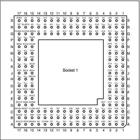
Socket 1
The original OverDrive socket, now officially called Socket 1, is a
169-pin PGA socket. Motherboards that have this socket can support any of the
486SX, DX, and DX2 processors and the DX2/OverDrive versions. This type of
socket is found on most 486 systems that originally were designed for OverDrive upgrades. Figure 3 shows the pinout
of Socket 1.
Figure 3. Intel Socket 1 pinout.
The original DX processor
draws a maximum 0.9 amps of 5V power in 33MHz form (4.5 watts) and a maximum 1
amp in 50MHz form (5 watts). The DX2 processor, or OverDrive
processor, draws a maximum 1.2 amps at 66MHz (6 watts). This minor increase in
power requires only a passive heatsink consisting of
aluminum fins that are glued to the processor with thermal transfer epoxy.
Passive heatsinks don't have any mechanical
components like fans. Heatsinks with fans or other
devices that use power are called active heatsinks. OverDrive processors
rated at 40MHz or less do not have heatsinks.
Socket 2
When the DX2 processor was
released, Intel was already working on the new Pentium processor. The company
wanted to offer a 32-bit, scaled-down version of the Pentium as an upgrade for
systems that originally came with a DX2 processor. Rather than just increasing
the clock rate, Intel created an all-new chip with enhanced capabilities
derived from the Pentium.
The chip, called the Pentium OverDrive processor, plugs into a processor socket with the
Socket 2 or Socket 3 design. These sockets hold any 486 SX, DX, or DX2 processor, as well as the Pentium OverDrive.
Because this chip is essentially a 32-bit version of the (normally 64-bit) Pentium
chip, many have taken to calling it a Pentium-SX. It was available in 25/63MHz
and 33/83MHz versions. The first number indicates the base motherboard speed;
the second number indicates the actual operating speed of the Pentium OverDrive chip. As you can see, it is a clock-multiplied
chip that runs at 2.5 times the motherboard speed. Figure 4 shows the pinout configuration of the official Socket 2 design.
Figure 4. 238-pin Intel Socket 2 configuration.

Notice that although the new
chip for Socket 2 is called Pentium OverDrive, it is
not a full-scale (64-bit) Pentium. Intel released the design of Socket 2 a
little prematurely and found that the chip ran too hot for many systems. The
company solved this problem by adding a special active heatsink
to the Pentium OverDrive processor. This active heatsink is a combination of a standard heatsink
and a built-in electric fan. Unlike the aftermarket glue-on or clip-on fans for
processors that you might have seen, this one actually draws 5V power directly
from the socket to drive the fan. No external connection to disk drive cables
or the power supply is required. The fan/heatsink
assembly clips and plugs directly into the processor and provides for easy
replacement if the fan fails.
Another requirement of the
active heatsink is additional clearance—no
obstructions for an area about 1.4'' off the base of the existing socket to
allow for heatsink clearance. The Pentium OverDrive upgrade is difficult or impossible in systems
that were not designed with this feature.
Another problem with this
particular upgrade is power consumption. The 5V Pentium OverDrive
processor draws up to 2.5 amps at 5V (including the fan) or 12.5 watts, which
is more than double the 1.2 amps (6 watts) drawn by the DX2 66 processor.
Note
Intel no longer markets OverDrive processors, but it maintains technical
information about them at http://www.intel.com/support/processors/overdrive/index.htm.
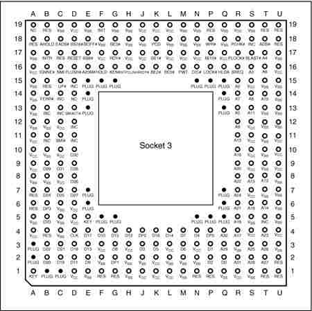
Socket 3
Because of problems with the
original Socket 2 specification and the enormous heat the 5V version of the
Pentium OverDrive processor generates, Intel came up
with an improved design. The new processor is the same as the previous Pentium OverDrive processor, except that it runs on 3.3V and draws
a maximum 3.0 amps of 3.3V (9.9 watts) and 0.2 amp of 5V (1 watt) to run the
fan—a total of 10.9 watts. This configuration provides a slight margin over the
5V version of this processor. The fan is easy to remove from the OverDrive processor for replacement, should it ever fail.
Intel had to create a new
socket to support both the DX4 processor, which runs on 3.3V,
and the 3.3V Pentium OverDrive processor. In addition
to the new 3.3V chips, this new socket supports the older 5V SX, DX, DX2, and
even the 5V Pentium OverDrive chip. The design,
called Socket 3, is the most flexible upgradeable 486 design. Figure 5 shows
the pinout specification of Socket 3.
Figure 5. 237-pin Intel Socket 3 configuration.
Notice that Socket 3 has one
additional pin and several others plugged in compared with Socket 2. Socket 3
provides for better keying, which prevents an end user from accidentally
installing the processor in an improper orientation. However, one serious
problem exists: This socket can't automatically determine the type of voltage
that is provided to it. You will likely find a jumper on the motherboard near
the socket to enable selecting 5V or 3.3V operation.
Caution
Because this jumper must be
manually set, however, a user could install a 3.3V processor in this socket
when it is configured for 5V operation. This installation instantly destroys
the chip when the system is powered on. So, it is up to the end user to ensure
that this socket is properly configured for voltage, depending on which type of
processor is installed. If the jumper is set in 3.3V configuration and a 5V
processor is installed, no harm will occur, but the system will not operate
properly unless the jumper is reset for 5V.
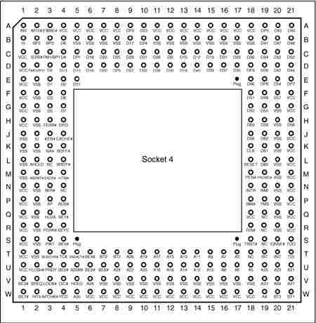
Socket 4
Socket 4 is a 273-pin socket
designed for the original Pentium processors. The original Pentium 60MHz and
66MHz version processors had 273 pins and plugged into Socket 4. It is a
5V-only socket because all the original Pentium processors run on 5V. This
socket accepts the original Pentium 60MHz or 66MHz processor and the OverDrive processor. Figure 6 shows the pinout
specification of Socket 4.
Figure 6. 273-pin Intel Socket 4 configuration.
Somewhat amazingly, the
original Pentium 66MHz processor consumes up to 3.2 amps of 5V power (16
watts), not including power for a standard active heatsink
(fan). The 66MHz OverDrive processor that replaced it
consumes a maximum 2.7 amps (13.5 watts), including about 1 watt to drive the
fan. Even the original 60MHz Pentium processor consumes up to 2.91 amps at 5V
(14.55 watts). It might seem strange that the replacement processor, which is
twice as fast, consumes less power than the original, but this has to do with
the manufacturing processes used for the original and OverDrive
processors.
Although both processors run
on 5V, the original Pentium processor was created with a circuit size of 0.8
micron, making that processor much more power-hungry than the 0.6-micron
circuits used in the OverDrive and the other Pentium
processors. Shrinking the circuit size is one of the best ways to decrease
power consumption. Although the OverDrive processor
for Pentium-based systems draws less power than the original processor,
additional clearance might have to be allowed for the active heatsink assembly that is mounted on top. As in other OverDrive processors with built-in fans, the power to run
the fan is drawn directly from the chip socket, so no separate power-supply connection
is required. Also, the fan is easy to replace should it ever fail.
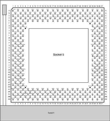
Socket 5
When Intel redesigned the
Pentium processor to run at 75MHz, 90MHz, and 100MHz, the company went to a
0.6-micron manufacturing process and 3.3V operation. This change resulted in
lower power consumption: only 3.25 amps at 3.3V (10.725 watts). Therefore, the
100MHz Pentium processor used far less power than even the original 60MHz
version. This resulted in lower power consumption and enabled the extremely
high clock rates without overheating.
The Pentium 75 and higher
processors actually have 296 pins, although they plug into the official Intel
Socket 5 design, which calls for a total of 320 pins. The additional pins are
used by the Pentium OverDrive for Pentium processors.
This socket has the 320 pins configured in a staggered PGA, in which the
individual pins are staggered for tighter clearance.
Several OverDrive
processors for existing Pentiums were available. These usually were later
design chips with integral voltage regulators to enable operating on the higher
voltages the older chips originally required. Intel no longer sells these;
however, companies such as Evergreen and PowerLeap do
still sell upgrade chips for older systems. Figure 7 shows the standard pinout for Socket 5.
Figure 7. 320-pin Intel Socket 5 configuration.
The Pentium OverDrive for Pentium processors has an active heatsink (fan) assembly that draws power directly from the
chip socket. The chip requires a maximum 4.33 amps of 3.3V to run the chip
(14.289 watts) and 0.2 amp of 5V power to run the fan (one watt), which results
in a total power consumption of 15.289 watts. This is less power than the
original 66MHz Pentium processor requires, yet it runs a chip that is as much
as four times faster!
Socket 6
The last 486 socket was
designed for the 486 DX4 and the 486 Pentium OverDrive processor. Socket 6 was intended as a
slightly redesigned version of Socket 3 and had an additional 2 pins plugged
for proper chip keying. Socket 6 has 235 pins and accepts only 3.3V 486 or OverDrive processors. Although Intel went to the trouble of
designing this socket, it never was built or implemented in any systems.
Motherboard manufacturers instead stuck with Socket 3.
Socket 7 (and
Super7)
Socket 7 is essentially the
same as Socket 5 with one additional key pin in the opposite inside corner of
the existing key pin. Socket 7, therefore, has 321 pins total in a 21x21 SPGA
arrangement. The real difference with Socket 7 is not with the socket itself,
but with the companion voltage regulator module (VRM) circuitry on the
motherboard that must accompany it.
The VRM is either a small
circuit board or a group of circuitry embedded in the motherboard that supplies
the proper voltage level and regulation of power to the processor.
The main reason for the VRM is
that Intel and AMD wanted to drop the voltages the processors would use from
the 3.3V or 5V supplied to the motherboard by the power supply. Rather than
require custom power supplies for different processors, the VRM converts the
3.3V or 5V to the proper voltage for the particular CPU you are using. Intel
released different versions of the Pentium and Pentium-MMX processors that ran
on 3.3V (called VR), 3.465V (called VRE), or 2.8V. Equivalent processors from
AMD, Cyrix, and others used voltages from 3.3V to 1.8V. Because of the variety
of voltages that might be required to support different processors, most
motherboard manufacturers started including VRM sockets or building adaptable VRMs into their Pentium motherboards.
Figure 8 shows the Socket 7 pinout.
Figure 8. Socket 7 (Pentium) pinout
(top view).
AMD, along with Cyrix and
several chipset manufacturers, pioneered an improvement or extension to the
Intel Socket 7 design called Super Socket 7 (or Super7), taking it from 66MHz
to 95MHz and 100MHz. This enabled faster Socket 7–type systems to be made,
supporting processors up to 500MHz, which are nearly as fast as some of the
newer Slot 1– and Socket 370–type systems using Intel processors. Super7
systems also have support for the AGP video bus, as well as Ultra DMA hard disk
controllers and advanced power management.
Major third-party chipset
suppliers including Acer Laboratories, Inc. (ALi);
VIA Technologies; and Silicon Integrated Systems (SiS)
all released chipsets for Super7 boards. Most of the major motherboard
manufacturers made Super7 boards in both Baby-AT and ATX form factors.
Socket 8
Socket 8 is a special SPGA
socket featuring a whopping 387 pins! This was specifically designed for the
Pentium Pro processor with the integrated L2 cache. The additional pins are to
enable the chipset to control the L2 cache integrated in the same package as
the processor. Figure 9 shows the Socket 8 pinout.
Figure 9. Socket 8 (Pentium Pro) pinout
showing power pin locations.
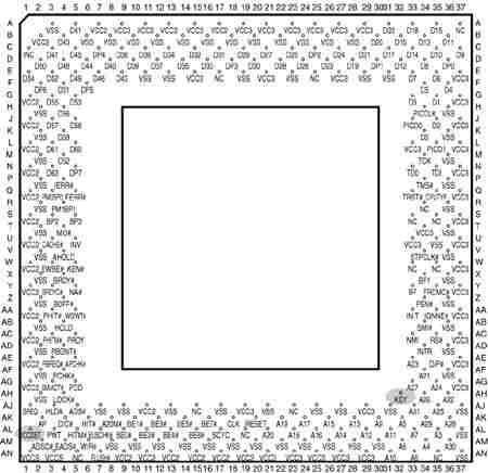
Socket 370
(PGA-370)
In January 1999, Intel
introduced a new socket for P6 class processors. The socket was called Socket
370 or PGA-370 because it has 370 pins and originally was designed for
lower-cost PGA versions of the Celeron and Pentium III processors. Socket 370
was originally designed to directly compete in the lower-end system market
along with the Super7 platform supported by AMD and Cyrix. However, Intel later
used it for the Pentium III processor. Initially all the Celeron and Pentium
III processors were made in SECC or SEPP format. These are essentially circuit
boards containing the processor and separate L2 cache chips on a small board
that plugs into the motherboard via Slot 1. This type of design was necessary
when the L2 cache chips were made a part of the processor but were not directly
integrated into the processor die. Intel did make a multiple-die chip package
for the Pentium Pro, but this proved to be a very expensive way to package the
chip, and a board with separate chips was cheaper, which is why the Pentium II
looks different from the Pentium Pro.
Starting with the Celeron 300A
processor introduced in August 1998, Intel began combining the L2 cache
directly on the processor die; it was no longer in separate chips. With the
cache fully integrated into the die, there was no longer a need for a
board-mounted processor. Because it costs more to make a Slot 1 board or
cartridge-type processor instead of a socketed type,
Intel moved back to the socket design to reduce the manufacturing
cost—especially with the Celeron, which at that time was competing on the low
end with Socket 7 chips from AMD and Cyrix.
The Socket 370 (PGA-370) pinout is shown in Figure 10.
Figure 10. Socket 370 (PGA-370) Pentium III/Celeron pinout (top view).
The Celeron was gradually
shifted over to PGA-370, although for a time both were available. All Celeron
processors at 333MHz and lower were available only in the Slot 1 version.
Celeron processors from 366MHz to 433MHz were available in both Slot 1 and
Socket 370 versions; all Celeron processors from 466MHz and up through 1.4GHz
are available only in the Socket 370 version.
Starting in October 1999,
Intel also introduced Pentium III processors with integrated cache that plug
into Socket 370. These use a packaging called flip chip pin grid array (FC-PGA),
in which the raw die is mounted on the substrate upside down. The slot version
of the Pentium III was more expensive and no longer necessary because of the
on-die L2 cache.
Note that because of some
voltage changes and one pin change, many original Socket 370 motherboards do
not accept the later FC-PGA Socket 370 versions of the Pentium III and Celeron.
Pentium III processors in the FC-PGA form have two RESET pins and require VRM
8.4 specifications. Prior motherboards designed only for the older versions of
the Celeron are referred to as legacy motherboards, and the newer motherboards supporting the
second RESET pin and VRM 8.4 specification are referred to as flexible
motherboards. Contact your motherboard or system manufacturer for
information to see whether your socket is the flexible version. Some
motherboards, such as the Intel CA810, do support the VRM 8.4 specifications
and supply proper voltage, but without Vtt support
the Pentium III processor in the FC-PGA package will be held in RESET#. The last
versions of the Pentium III and Celeron III use the Tualatin core design, which
also requires a revised socket to operate. Motherboards that can handle
Tualatin-core processors are known as Tualatin-ready
and use different chipsets from those not designed to work with the
Tualatin-core processor. Companies that sell upgrade processors offer products
that enable you to install a Tualatin-core Pentium III or Celeron III processor
into a motherboard that lacks built-in Tualatin support.
Installing a Pentium III
processor in the FC-PGA package into an older motherboard is unlikely to damage
the motherboard. However, the processor itself could be damaged. Pentium III
processors in the 0.18-micron process operate at either 1.60V or 1.65V, whereas
the Intel Celeron processors operate at 2.00V. The motherboard could be damaged
if the motherboard BIOS fails to recognize the voltage identification of the
processor. Contact your PC or motherboard manufacturer before installation to
ensure compatibility.
A motherboard with a Slot 1
can be designed to accept almost any Celeron, Pentium II, or Pentium III
processor. To use the socketed Celerons and Pentium
III processors, several manufacturers have made available a low-cost
slot-to-socket adapter sometimes called a slot-ket. This is essentially a Slot 1 board containing
only a Socket 370, which enables you to use a PGA processor in any Slot 1
board.
Socket 423
Socket 423 is a ZIF-type
socket introduced in November 2000 for the original Pentium 4. Figure 11 shows
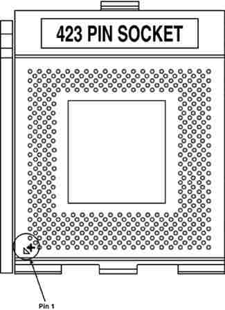
Socket 423.
Figure 11. Socket 423 (Pentium 4) showing pin 1 location.
Socket 423 supports a 400MHz
processor bus, which connects the processor to the Memory Controller Hub (MCH),
which is the main part of the motherboard chipset and similar to the
Socket 423 uses a unique heatsink mounting method that requires standoffs attached
either to the chassis or to a special plate that mounts underneath the
motherboard. This was designed to support the weight of the larger heatsinks required for the Pentium 4. Because of this, many
Socket 423 motherboards require a special chassis that has the necessary
additional standoffs installed. Fortunately, the need for these standoffs was
eliminated with the newer Socket 478 for Pentium 4 processors.
The processor uses five
voltage ID (VID) pins to signal the VRM built into the motherboard to deliver
the correct voltage for the particular CPU you install. This makes the voltage
selection completely automatic and foolproof. Most Pentium 4 processors for
Socket 423 require 1.7V. A small triangular mark indicates the pin-1 corner for
proper orientation of the chip.
Socket 478
Socket 478 is a ZIF-type
socket for the Pentium 4 and Celeron 4 (Celerons based on the Pentium 4 core)
introduced in October 2001. It was specially designed to support additional
pins for future Pentium 4 processors and speeds over 2GHz. The heatsink mounting is different from the previous Socket
423, allowing larger heatsinks to be attached to the
CPU. Figure 12 shows Socket 478.
Figure 12. Socket 478 (Pentium 4) showing pin 1 location.

Socket 478 supports a 400MHz,
533MHz, or 800MHz processor bus that connects the processor to the memory
controller hub (MCH), which is the main part of the motherboard chipset.
Socket 478 uses a new heatsink attachment method that clips the heatsink directly to the motherboard, and not the CPU
socket or chassis (as with Socket 423). Therefore, any standard chassis can be
used, and the special standoffs used by Socket 423 boards are not required. The
new heatsink attachment allows for a much greater
clamping load between the heatsink and processor,
which aids cooling.
Socket 478 processors use five
VID pins to signal the VRM built into the motherboard to deliver the correct
voltage for the particular CPU you install. This makes the voltage selection
completely automatic and foolproof. A small triangular mark indicates the pin-1
corner for proper orientation of the chip.
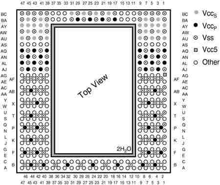
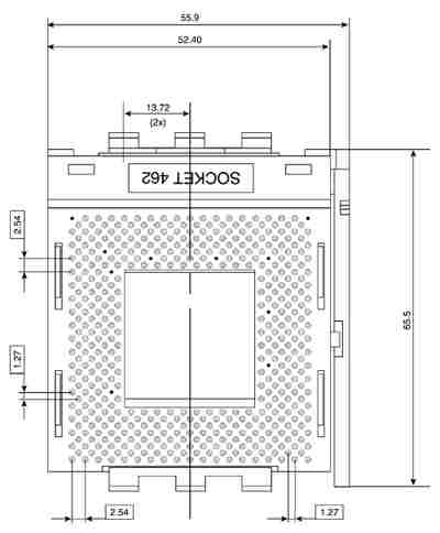
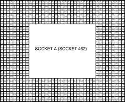
Socket A (Socket 462)
AMD introduced Socket A, also called Socket 462, in June 2000 to support the PGA
versions of the Athlon and Duron
processors. It is designed as a replacement for Slot A used by the original Athlon processor. Because the Athlon
has now moved to incorporate L2 cache on-die, and the new low-cost Duron is available only in an on-die cache version, there
was no longer a need for the expensive cartridge packaging the original Athlon processors used.
Socket A has 462 pins and 11
plugs oriented in an SPGA form (see Figure 13). Socket A has the same physical
dimensions and layout as Socket 370; however, the location and placement of the
plugs prevent Socket 370 processors from being inserted. Socket A supports 32 voltage levels from 1.100V to 1.850V in 0.025V
increments, controlled by the VID0-VID4 pins on the processor. The automatic
voltage regulator module circuitry typically is embedded on the motherboard.
Figure 13. Socket A (Socket 462) Athlon/Duron layout.
There are 11 total plugged
holes, including 2 of the outside pin holes at A1 and AN1. These are used to
allow for keying to force the proper orientation of the processor in the
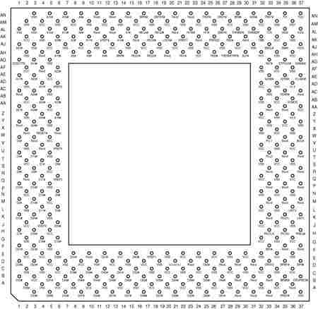
socket. The pinout of Socket A is shown in Figure 14.
Figure 14. Socket A (Socket 462) Athlon/Duron pinout (top view).
After the introduction of
Socket A, AMD moved all Athlon (including all Athlon XP) processors to this form factor, phasing out Slot
A. In addition, for a time AMD also sold a reduced L2 cache version of the Athlon called the Duron in this
form factor. The Athlon 64 uses a different processor
socket called Socket 754.
Caution
Just because a chip can plug
into a socket doesn't mean it will work. The newer Athlon
XP processors require different voltages, BIOS, and chipset support than
earlier Socket A Athlon and Duron processors. As always, make sure your motherboard
supports the processor you intend to install.
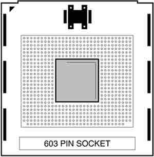
Socket 603
Socket 603 is used with the
Intel Xeon processor in DP (dual processor) and MP (multiple processor)
configurations. These are typically used in motherboards designed for use in
network file servers. Figure 15 shows Socket 603.
Figure 15. Socket 603 is used by the Intel Xeon processor.
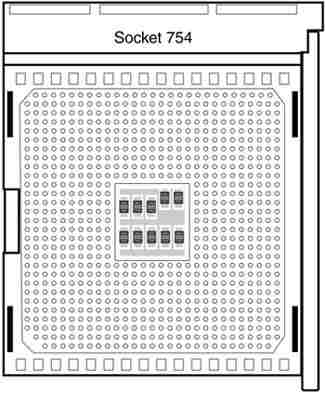
Socket 754
Socket 754 is used with the
new AMD Athlon 64 processor, which is AMD's first
64-bit processor for desktop computers. Figure 16 shows an overhead view of
this socket.
Figure 16. Socket 754. The large
cutout corner at the lower left indicates pin 1.
Processor Slots
After introducing the Pentium
Pro with its integrated L2 cache, Intel discovered that the physical package it
chose was very costly to produce. Intel was looking for a way to easily
integrate cache and possibly other components into a processor package, and it
came up with a cartridge or board design as the best way to do this. To accept
its new cartridges, Intel designed two types of slots that could be used on
motherboards.
Slot 1 is a 242-pin slot
designed to accept Pentium II, Pentium III, and most Celeron processors. Slot
2, on the other hand, is a more sophisticated 330-pin slot designed for the
Pentium II Xeon and Pentium III Xeon processors, which are primarily for
workstations and servers. Besides the extra pins, the biggest difference
between Slot 1 and Slot 2 is the fact that Slot 2 was designed to host up to
four-way or more processing in a single board. Slot 1 allows only single or
dual processing functionality.
Note that Slot 2 is also
called SC330, which stands for slot connector with 330 pins. Intel later
discovered less-expensive ways to integrate L2 cache into the processor core
and no longer produces Slot 1 or Slot 2 processors. Both Slot 1 and Slot 2
processors are now obsolete, and many systems using these processors have been
retired or upgraded with socket-based motherboards.
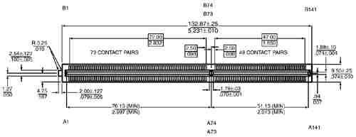
Slot 1 (SC242)
Slot 1, also called SC242
(slot connector 242 pins), is used by the SEC design that is used with the
cartridge-type Pentium II/III and Celeron processors (see Figure 17).
Figure 17. Slot 1 connector dimensions and pin layout.
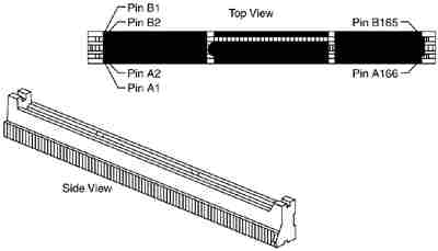
Slot 2 (SC330)
Slot 2, otherwise called SC330
(slot connector 330 pins), is used on high-end motherboards that support the
Pentium II and III Xeon processors. Figure 18 shows the Slot 2 connector.
Figure 18. Slot 2 (SC330) connector dimensions and pin layout.
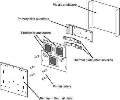
The Pentium II Xeon and
Pentium III Xeon processors are designed in a cartridge similar to, but larger
than, that used for the standard Pentium II/III. Figure 19 shows the Xeon
cartridge.
Figure 19. Pentium II/III Xeon cartridge.
Slot 2 motherboards were used in
higher-end systems such as workstations or servers based on the Pentium II Xeon
or Pentium III Xeon. These versions of the Xeon differ from the standard
Pentium II and slot-based Pentium III mainly by virtue of having full-core
speed L2 cache, and in some versions more of it. The additional pins allow for
additional signals needed by multiple processors.